
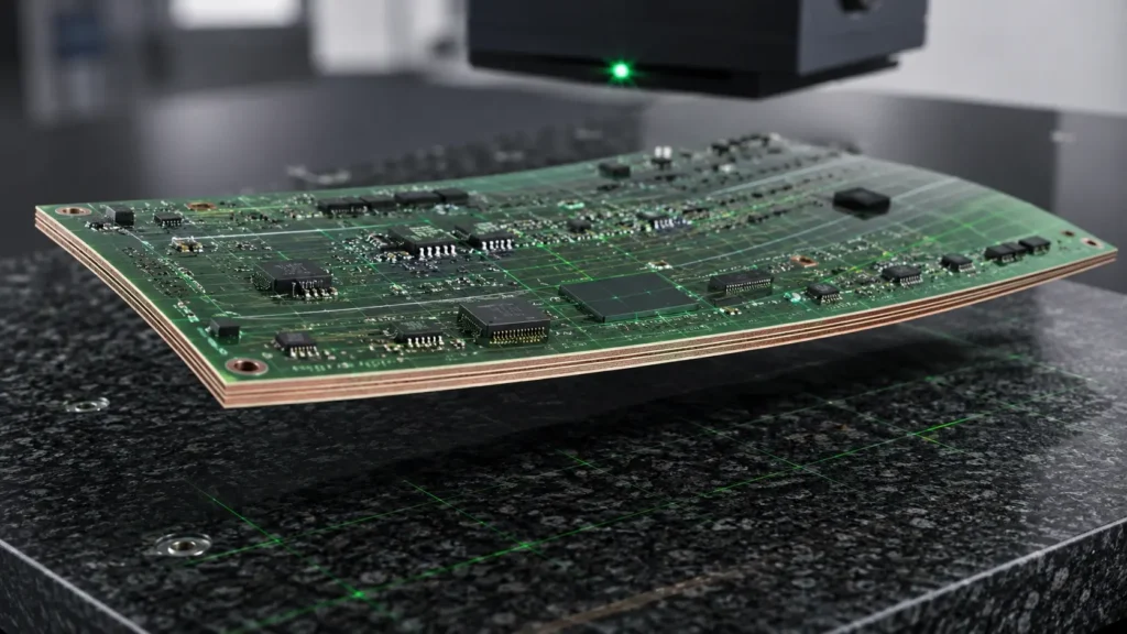
A finished PCB can pass electrical test and still create a production problem because it does not remain flat. A lifted edge may interfere with stencil contact, placement support, connector alignment, enclosure assembly, or a thermal interface. For thin, large, asymmetric, or densely populated boards, the issue can become more visible after reflow than it was at incoming inspection.
Reliable PCB manufacturing therefore treats bow and twist as product characteristics, not cosmetic defects. The team must agree what object is controlled—the individual board or the assembly panel—when it is measured, how it is supported, which revision and stack-up apply, and what requirement governs acceptance. These decisions should be discussed with the PCB fabrication supplier before the construction is frozen.
Start with the functional consequence: A board does not need to look perfectly flat in a photograph. It needs to meet the agreed flatness requirement under the agreed measurement condition and still fit the printing, placement, soldering, mechanical, connector, and thermal processes that matter to the product.
1. Bow and Twist Describe Different Shapes
Bow is a roughly cylindrical or spherical curvature in which the board departs from a plane while its corners remain broadly aligned. Twist is a diagonal deformation in which one or more corners move out of the plane defined by the others. A real board can contain both.
This distinction matters because length, width, diagonal, support condition, and maximum vertical displacement enter the measurement differently. A statement such as “the board is warped by 1 mm” is incomplete without the board dimensions, shape type, test method, and measurement state.
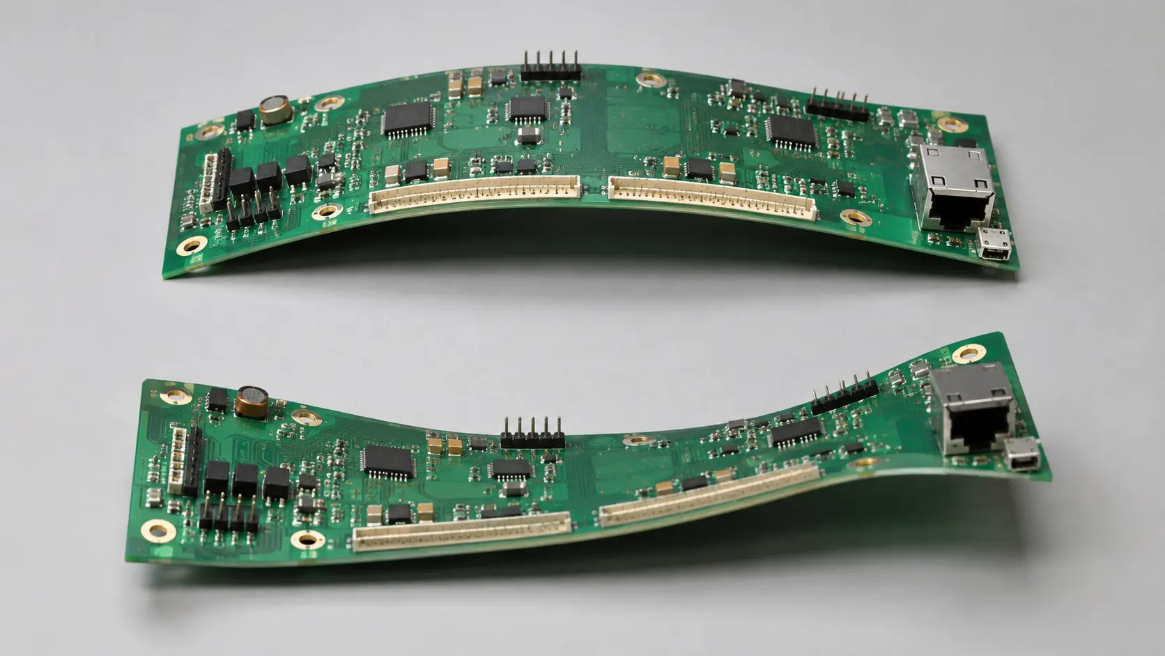
Measurement warning: Do not press a board flat, take a convenient gap reading, and report that value as free-state warpage. Use the specified method consistently. Record board orientation, dimensions, temperature or preconditioning state, fixture, support, measured displacement, calculation, and result.
2. Warpage Usually Comes from an Imbalance
A printed board is a bonded structure of copper, resin, reinforcement, surface coatings, and sometimes dissimilar materials. During lamination, cooling, plating, solder-mask curing, profiling, storage, and assembly heating, these parts do not respond identically. Curvature appears when shrinkage, expansion, stiffness, moisture, or process stress is not balanced through the thickness or across the area.
Common contributors include an asymmetric layer stack, large copper planes concentrated on one side, major differences in copper density between opposing layers, unsuitable prepreg or resin-flow conditions, uneven heating or cooling, thin residual webs around cutouts, an unbalanced panel layout, and mechanical handling. None of these factors proves the root cause by itself. A useful investigation compares design data, material lot, press cycle, panel position, process history, and the shape of the measured deformation.
| Possible contributor | Evidence worth reviewing | Practical control direction |
|---|---|---|
| Asymmetric stack-up | Copper, dielectric, material, and thickness mirrored around the center | Review construction before routing is locked |
| Copper imbalance | Layer images, plane coverage, heavy copper regions, copper thieving strategy | Balance opposing layers where function permits |
| Lamination and cooling | Material set, press recipe, resin flow, panel location, cooling history | Use a qualified construction and controlled cycle |
| Panel and profiling stress | Rail geometry, routing sequence, V-score, tab locations, residual webs | Design a mechanically balanced panel and depaneling method |
| Storage or moisture | Packaging, time, environment, preconditioning, change before and after heat | Control handling and define the measurement state |
| Assembly heating | Reflow profile, fixture support, component distribution, hot spots | Evaluate the assembled process, not only the incoming bare board |
3. Design the Stack-Up and Copper Distribution Together
Layer count should not be selected independently from flatness risk. The 2-layer, 4-layer, and multilayer PCB guide explains why signal, plane, dielectric, and mechanical requirements must be considered as one construction. A geometrically symmetric stack is a strong starting point, but symmetry in layer names is not enough if copper coverage and local stiffness remain strongly unbalanced.
Large solid planes on one side and sparse routing on the opposing side can create different process responses. Copper balancing or thieving may help in suitable areas, but it must not compromise controlled impedance, creepage, isolation, antennas, current paths, or thermal design. The fabricator should review the actual production artwork rather than applying an automatic copper pattern without agreement.
Material properties and finished thickness also affect stiffness and thermal response. The PCB material selection guide explains why FR-4, high-Tg, high-frequency, and metal-based constructions are not interchangeable labels. When different materials or copper weights are combined, the construction should be reviewed for manufacturability and thermal compatibility.
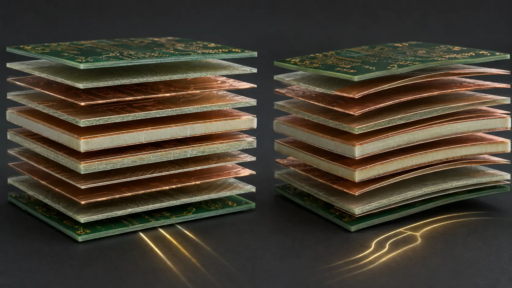
Common mistake: Fixing overall thickness and layer count, then allowing large copper or dielectric changes without another mechanical review. Stack-up revisions affect more than impedance and cost; they can change resin demand, stiffness, thermal response, finished thickness, and flatness.
4. The Panel Can Behave Differently from the Board
An individual board may be acceptable after depaneling while the production array does not sit correctly on stencil tooling, a conveyor, or a placement support. The reverse can also happen: rails temporarily restrain the panel, and deformation becomes visible only after routing or V-scoring releases the parts.
The PCB panelization guide covers rails, V-score, mouse bites, tooling features, and SMT handling. For flatness control, also review board orientation, mixed designs, copper distribution, rail width, breakaway geometry, large cutouts, routing sequence, and whether acceptance applies to the array, the individual board, or both.
Do not assume that a finished-board requirement automatically defines the panel requirement. IPC application addenda illustrate that array requirements may need agreement between user and supplier. Put the controlled object and measurement stage directly in the procurement documentation.
5. Measure Bow and Twist with a Defined Method
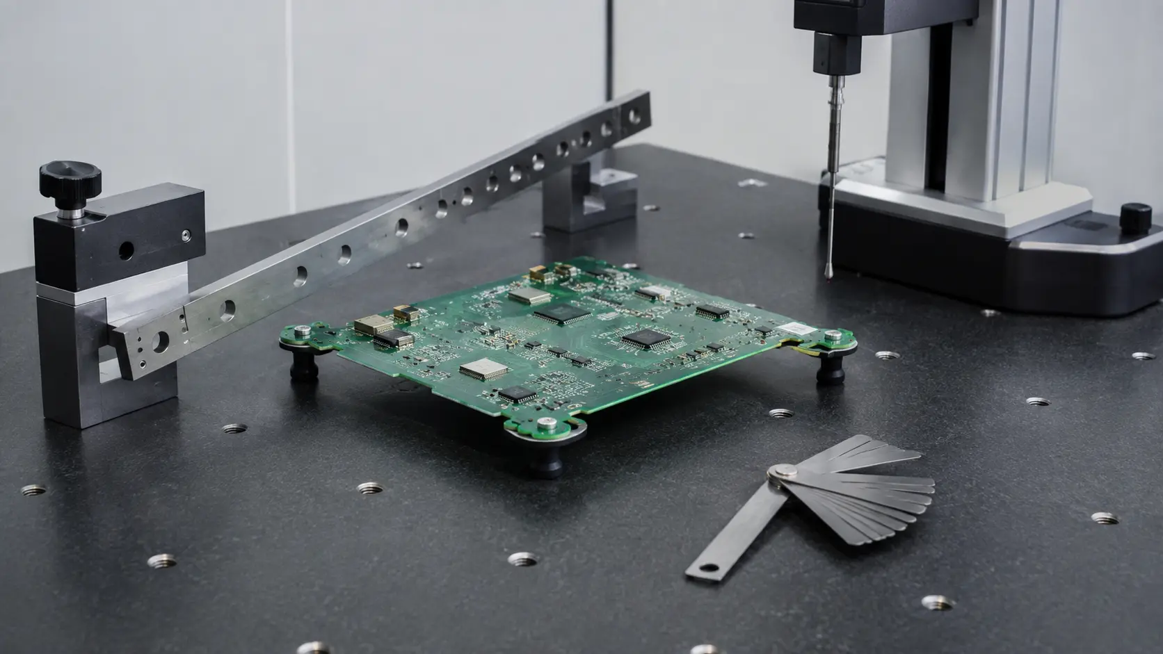
IPC lists IPC-TM-650 Method 2.4.22C as “Bow and Twist (Percentage).” The published method uses board dimensions and vertical displacement to determine bow or twist percentage. It also distinguishes the techniques used for the two shapes.
The method explains how to place the sample on a flat reference surface, establish the relevant dimension, determine displacement, and calculate a percentage. The percentage allows boards of different sizes to be compared more meaningfully than a gap value alone. The acceptance limit, however, must come from the applicable product specification and procurement agreement.
| Release question | Why it matters | Record to retain |
|---|---|---|
| What is measured? | Panel and individual board may behave differently | Part number, panel drawing, sample location |
| When is it measured? | Incoming, after conditioning, after depaneling, and after reflow are different states | Process stage, time, environment, thermal history |
| Which method applies? | Support and calculation affect the result | Method revision, fixture, dimensions, raw readings |
| What is the limit? | Requirements vary by product, array, class, addendum, and agreement | Specification clause and customer exception |
| What happens after failure? | Flattening may hide cause without proving process stability | Disposition, root-cause evidence, corrective action |
6. Flatness Problems Often Appear During Assembly
During PCB assembly, warpage can reduce stencil gasketing, change paste transfer, prevent consistent vacuum support, shift component height relative to the placement head, or create uneven contact with pallets and fixtures. After reflow, the board must still align with connectors, screws, card guides, housings, displays, heat spreaders, and thermal interface materials.
For BGA and other bottom-terminated components, board and package warpage interact during heating and cooling. X-ray can help inspect hidden joints, but it does not by itself prove that board flatness caused an observed defect. Correlate incoming measurements, reflow profile, fixture condition, joint evidence, panel position, and component data. The PCB assembly testing and inspection guide explains the limits of common methods.
Buyer takeaway: A supplier report stating “flatness passed” is useful only when it identifies the board or array, revision, sample quantity, measurement state, method, raw dimensions, calculated result, requirement, and disposition. Ask for traceable evidence when flatness is functionally critical.
7. Build Flatness into the Release Package
IPC-6012F places bow and twist within printed-board dimensional requirements. Confirm the active document through the IPC revision table, then state the applicable class, addendum, exceptions, sampling, preconditioning, panel requirement, and evidence in the procurement package.
The release package should include the approved stack-up, material requirements, finished thickness, copper by layer, panel drawing, profiling method, critical mechanical interfaces, flatness requirement, measurement method and stage, and authorization path for deviations. When the product is sensitive to reflow or enclosure fit, include the assembly profile, fixture concept, and functional interface drawing.
Reliable flatness does not come from a final inspection alone. It is the result of coordinated stack-up design, copper distribution, material choice, lamination, panelization, thermal history, handling, measurement, and assembly planning.
EazyPCB supports PCB fabrication, stack-up review, panelization, prototypes, flatness coordination, PCBA assembly, and production. To review a project, contact EazyPCB with PCB data, stack-up, panel drawing, material and thickness requirements, assembly files, enclosure interfaces, quantity, and required inspection evidence.
