
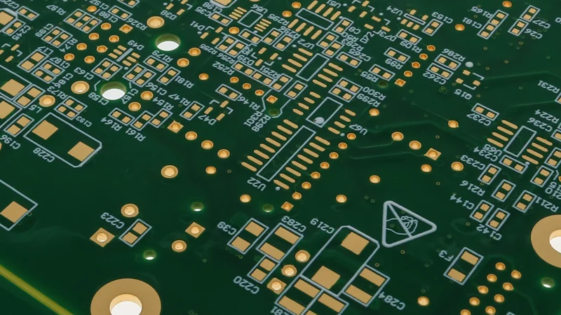
Solder mask is the protective coating applied over the copper surface of a PCB. It helps prevent solder bridges, protects copper from oxidation, improves insulation, and gives the board its familiar green, blue, red, black, white, or other color.
Although solder mask looks like a simple surface layer, it plays an important role in PCB fabrication and SMT assembly. Poor solder mask design can cause soldering defects, exposed copper, assembly problems, and production delays.
What Is PCB Solder Mask?
PCB solder mask is an insulating polymer layer that covers most of the copper traces and copper pours. Only the areas that need soldering, electrical contact, or testing are exposed through solder mask openings.
The solder mask layer is included in the Gerber file package. Before production, it is important to confirm that solder mask openings, pads, vias, fiducials, test points, and special copper areas are correctly defined.
Solder Mask Color: Does It Matter?
Green is the most common solder mask color because it is stable, easy to inspect, and widely used in PCB production. Other colors such as blue, red, black, white, yellow, and matte black are also available for branding, visual preference, or product appearance.
Color can affect visual inspection and contrast. For example, white solder mask is often used for LED boards because it reflects light, while black solder mask can look premium but may be harder to inspect. If your board has dense SMT assembly or fine-pitch components, inspection visibility should be considered.
Solder Mask Clearance
Solder mask clearance is the opening around a pad where the solder mask is removed. If the opening is too small, it may cover part of the pad and affect solderability. If it is too large, it may expose too much copper and increase solder bridge risk.
For reliable manufacturing, solder mask clearance should match the manufacturer’s process capability. A complete Gerber file checklist helps catch missing or incorrect solder mask layers before ordering.
Solder Mask Dam Between Pads
A solder mask dam is the narrow strip of solder mask between adjacent pads. It helps reduce solder bridging, especially for ICs, connectors, and fine-pitch SMT components.
However, if pads are too close together, the solder mask dam may be too narrow to manufacture reliably. In this case, the manufacturer may need to remove the mask dam or adjust the design. This is a common DFM point for fine-pitch components.
Via Tenting, Plugging, and Filling
Via tenting means covering a via with solder mask. It can help prevent solder from flowing into the via during assembly and can reduce the chance of contamination. Small vias are often tented by default, depending on the design and manufacturer rules.
For via-in-pad, high-reliability assemblies, or BGA areas, simple tenting may not be enough. Plugged, filled, or capped vias may be required to prevent solder wicking and voids. These requirements should be clearly stated before production.
Solder Mask and Surface Finish
Solder mask defines which copper areas remain exposed for surface finish. ENIG, HASL, OSP, immersion silver, and immersion tin are applied only to exposed solderable areas, not to copper covered by solder mask.
If you are choosing a finish, see our guide on PCB surface finish options. Solder mask design and surface finish should be reviewed together for fine-pitch pads, test points, edge connectors, and assembly reliability.
Common Solder Mask Problems
- Solder mask opening covers part of the pad.
- Excessive clearance exposes too much copper.
- Missing solder mask dam causes solder bridges.
- Vias are not tented or plugged as expected.
- Silkscreen overlaps exposed solderable areas.
- Solder mask color makes inspection more difficult.
DFM Tips for Solder Mask
Solder mask should be reviewed as part of the overall PCB DFM process. Check pad openings, mask slivers, fine-pitch areas, via treatment, solderable copper, and any special process notes before production.
Our PCB DFM checklist explains more design points that should be reviewed before fabrication. For quality expectations, the IPC standards family is widely used in PCB manufacturing, and IPC-A-600 is commonly associated with acceptability of printed boards.
Prepare Solder Mask Data Carefully
A good solder mask design helps improve soldering quality, inspection, appearance, and long-term reliability. It is especially important for fine-pitch SMT, BGA, via-in-pad, high-density PCB, and production projects.
EazyPCB supports prototype and production PCB projects with engineering review and quality control. If you are unsure about solder mask clearance, via tenting, or fine-pitch DFM, you can contact our team before releasing files for manufacturing.
