
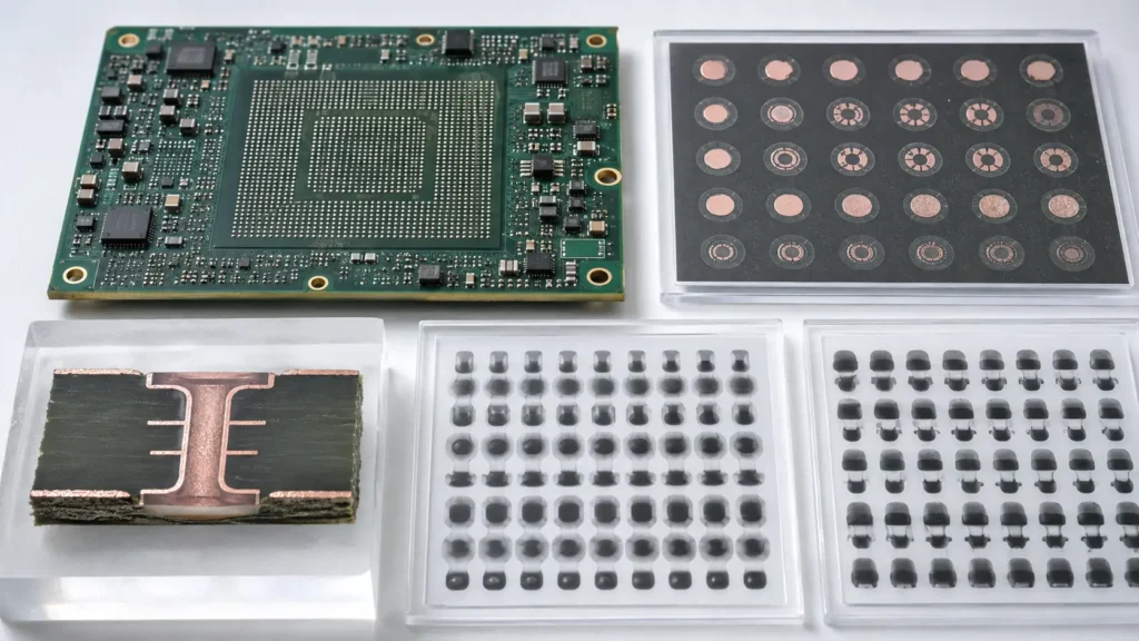
A via placed inside a component pad can solve a difficult routing problem and create a short electrical or thermal path. It can also create a soldering problem if the fabrication drawing merely says “via-in-pad” and leaves the protection method undefined.
Reliable PCB manufacturing starts by treating via-in-pad as a complete structure: via type, layer span, plated barrel, fill material, surface preparation, copper cap, final finish, pad geometry, assembly process, and acceptance evidence. The need for that structure should be confirmed before the layout is frozen with the PCB fabrication supplier and assembly team.
Decision gate: Use via-in-pad because the package escape, current path, thermal path, or RF geometry needs it—not because it looks cleaner in CAD. If an ordinary dog-bone fan-out meets the product requirements, it may avoid extra fabrication steps and inspection controls.
1. What Via-in-Pad Changes
In a conventional fan-out, a short trace connects the component land to a nearby via. With via-in-pad, the via opening is placed within the solderable land. This can release routing space beneath fine-pitch BGA and wafer-level packages, reduce interconnect length, connect a thermal pad to internal copper, or help a dense HDI PCB escape from the top layer.
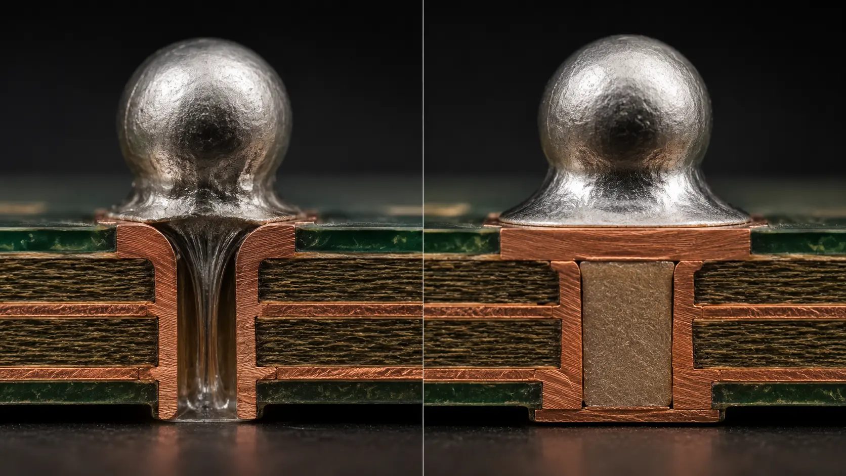
The same geometry creates a direct path from the assembly pad into the via barrel. If that path remains open or depressed, solder paste may move into the via, the available solder volume may change, and the joint may not sit on a uniform surface. The risk depends on package, pad, via, stencil, finish, reflow, and acceptance criteria; it should not be reduced to one universal via diameter.
2. Tented, Plugged, Filled, and Capped Are Not Synonyms
IPC-4761 organizes via protection into distinct types, including tented, plugged, filled, filled and covered, and filled and capped structures. Its public table of contents also identifies planarity, metallization, voids, separation, materials, and drawing notes as separate considerations. The terminology matters because each construction leaves a different pad surface and follows a different process.
| Description used in a project | What it normally controls | Why it may be insufficient under a solder pad |
|---|---|---|
| Open via | No added closure | Provides a path for solder, flux, or process chemistry |
| Tented or covered | Solder mask protection over an opening | Does not by itself create a solid, planar copper land |
| Plugged | Material placed partly into the via | Fill depth, surface shape, and coverage still need definition |
| Filled | Via barrel filled with an agreed material | A filled surface is not automatically planarized and copper capped |
| Filled and capped | Filled structure with secondary metallization across both ends | Still requires agreed geometry, planarity, finish, inspection, and supplier capability |
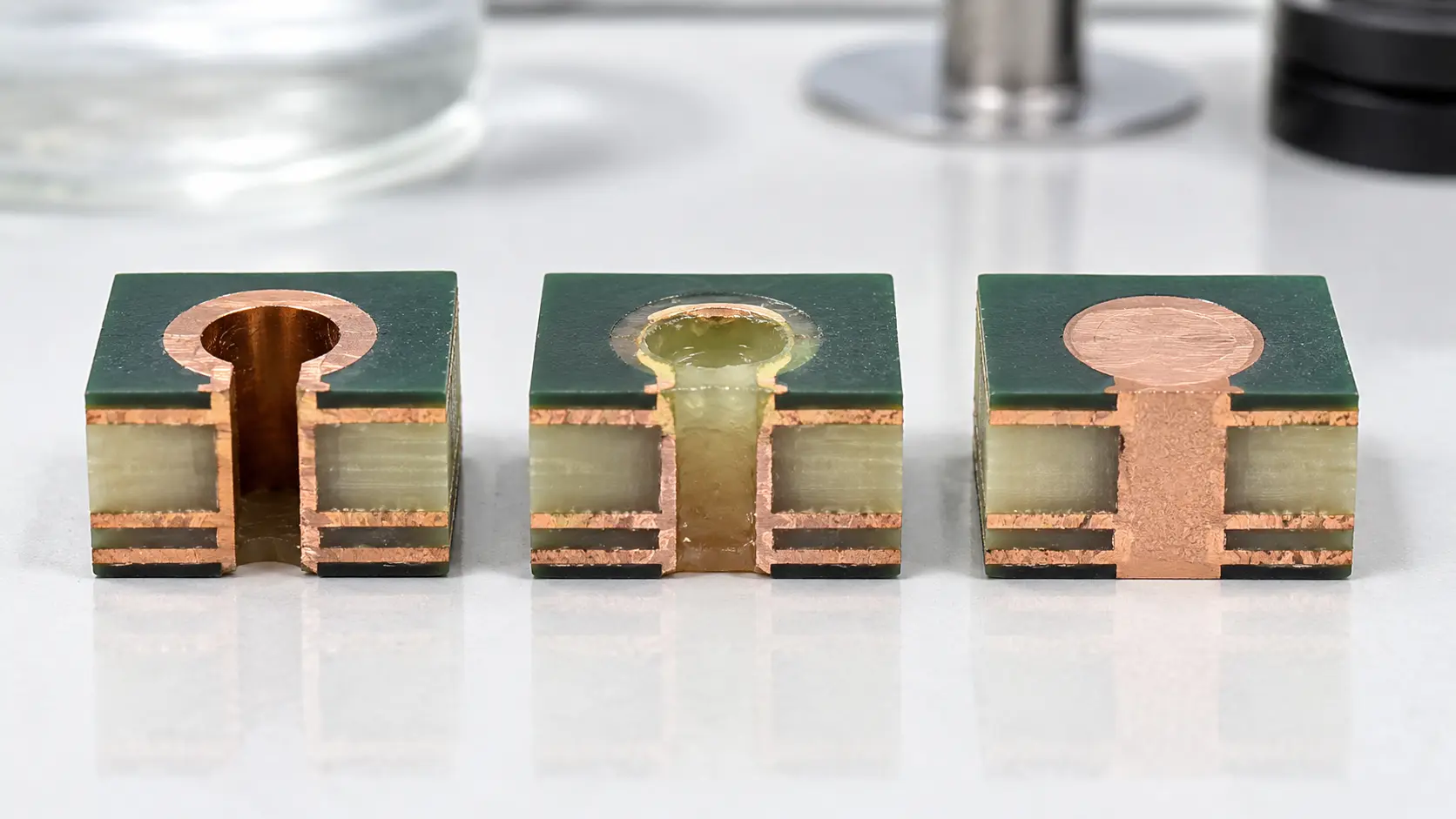
Terminology warning: “Plug the vias” is not a complete via-in-pad note. Identify the applicable protection type or construction, which vias it applies to, the required finished surface, and the acceptance document. A verbal agreement during quotation should be transferred into the released package.
3. Why Type VII Is Commonly Referenced
An IPC technical resource derived from IPC-4761 states that Type VII filled and capped via protection is recommended when specifying via-in-pad. In practical terms, the plated via is filled, the surface is prepared, and secondary metallization covers the via ends so the component land can be formed over the structure.
That reference is useful, but writing only “IPC-4761 Type VII” does not finish the design work. The team still needs to identify the via population, layer span, pad and mask geometry, fill system, finished surface expectation, applicable product specification, and inspection evidence. Any requirement from the component supplier remains part-specific.
Infineon’s high-density BGA layout examples use via-in-pad technology and explicitly call for a flat surface at the top land. Analog Devices similarly notes in its wafer-level package guidance that a dimple at a via-in-pad can contribute to solder voiding and that a completely flat surface can be achieved through capping. These examples support a simple rule: follow the exact package documentation and agree the board construction with the fabricator.
4. The Manufacturing Sequence Must Produce One Pad
A filled and capped via is made through a controlled sequence rather than a single “plugging” operation. The exact route depends on board construction, via type, materials, and supplier process, but the engineering logic is consistent:
- Create and metallize the via according to the approved layer structure.
- Prepare the barrel and apply the qualified fill material with adequate penetration.
- Cure the fill using a controlled process compatible with subsequent thermal steps.
- Remove excess material and planarize the surface without damaging the surrounding copper.
- Apply the secondary copper metallization that closes the ends and supports the final pad.
- Complete patterning, solder mask, surface finish, and inspection as required by the released design.
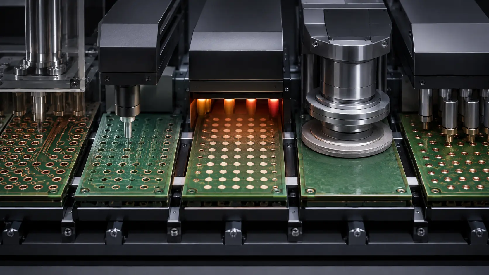
Defects can originate at the interfaces between these stages. Examples include incomplete fill, voids, separation between fill and hole wall, a depression or bump at the surface, damage during planarization, or an unsuitable cap. The solution is not a generic “zero void” claim copied into every purchase order. Define the applicable workmanship and performance documents, sampling plan, and evidence according to product risk.
Common mistake: Adding via-in-pad late to rescue BGA routing after the stack-up and quotation are fixed. The change can affect drill strategy, lamination sequence, fill process, outer-layer imaging, pad planarity, cost, lead time, assembly setup, and inspection. Review it as a construction change, not a cosmetic layout edit.
5. Planarity Belongs to Both Fabrication and Assembly
The bare-board drawing defines the finished pad, but the consequence appears during PCB assembly. A local depression may change solder-paste support or joint geometry. A protrusion may affect stencil contact or component seating. A missing cap can allow solder movement into the via. The final result also depends on stencil design, paste, placement, reflow profile, package warpage, pad finish, and the component manufacturer’s land-pattern guidance.
For signal vias, via-in-pad can also interact with layer transitions, return paths, and stubs. The controlled impedance PCB guide provides wider context, but the specific transition still requires signal-integrity review. For thermal pads, do not assume conductive fill is automatically the best answer; thermal performance, material compatibility, reliability, and manufacturing capability must be evaluated as a system.
6. What to Put in the Release Package
A quotation can begin with CAD data and a short note, but production release needs one unambiguous package. Mark the affected vias consistently in the drill data, fabrication drawing, stack-up, pad geometry, and any separate via table. Do not rely on color, an informal screenshot, or an email attachment that is not revision controlled.
| Release item | Question it must answer | Typical ambiguity to remove |
|---|---|---|
| Via identification | Which exact vias receive the special process? | All vias, only BGA vias, or only named nets |
| Structure | Through, blind, buried, microvia, stacked, or staggered? | Layer span and lamination stage |
| Protection and finish | Filled, planarized, capped, and finished how? | Plugging confused with full fill and cap |
| Pad interface | What land, mask, and package rules control assembly? | Generic library footprint used instead of package guidance |
| Acceptance evidence | How will fill, cap, planarity, and assembly be verified? | “Inspect as normal” without a defined result |
| Revision control | Do every file and note describe the same build? | Via table updated without regenerating production data |
Buyer takeaway: Ask for evidence, not adjectives. “Premium via fill” cannot be inspected. An agreed construction, drawing note, revision, inspection method, sample location, and acceptance record can.
7. Inspect the Structure at the Right Stages
Surface inspection can check pad condition and local topography, but it cannot reveal every internal fill or barrel condition. Depending on risk and specification, evidence may include process records, optical measurement, microsection analysis, electrical test, X-ray of the assembled BGA, and functional verification. The broader PCB assembly testing and inspection guide explains what common methods can and cannot prove.
Inspection depth should follow consequence. A via-in-pad used only to gain routing space does not necessarily require the same evidence as a via carrying heat from a power package or forming a critical high-speed transition. Define the failure concern first, then select the evidence that can actually detect it.
Final Thoughts
Via-in-pad is valuable when it solves a real density, electrical, or thermal constraint. Its reliability does not come from placing a via at the center of a pad; it comes from coordinating package guidance, stack-up, via geometry, fill, planarization, copper capping, finish, assembly, and inspection.
EazyPCB supports PCB fabrication, HDI review, via-in-pad coordination, prototyping, PCBA assembly, and production. To review a project, contact EazyPCB with the released PCB data, stack-up, fabrication drawing, package drawing, via table, assembly files, quantity, and required acceptance evidence.
