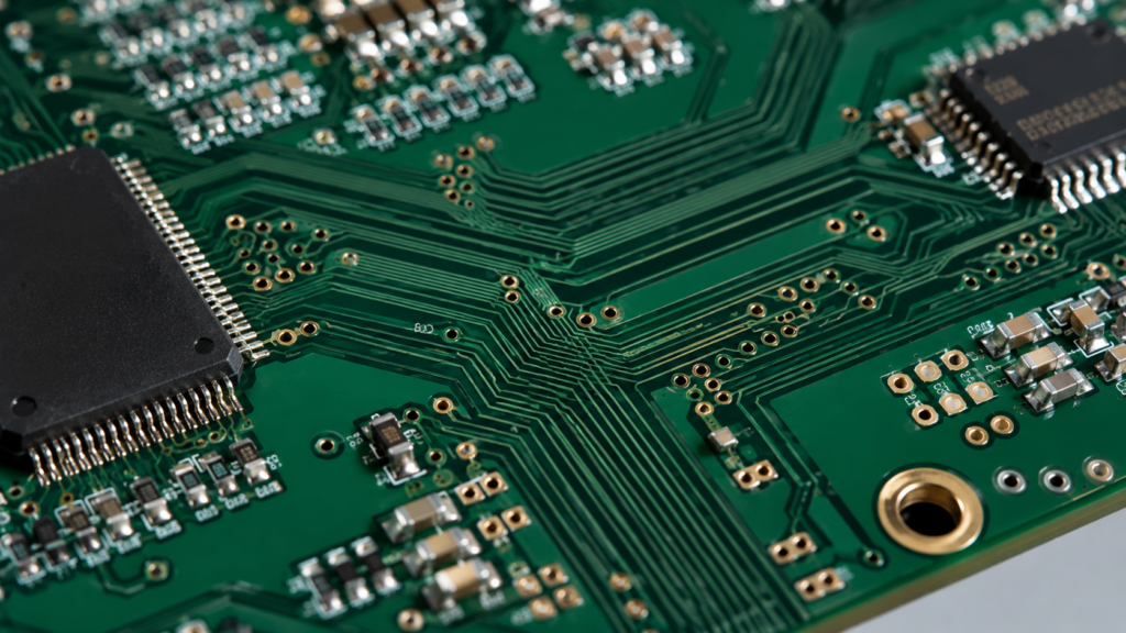
Controlled impedance PCB design is important when signals travel fast enough that the PCB trace behaves like a transmission line instead of a simple connection. In high-speed circuits, the geometry of the trace, the dielectric material, and the reference plane all affect signal quality.
If impedance is not controlled, signals may suffer from reflections, ringing, timing errors, data loss, EMI issues, and unreliable product performance. This is why controlled impedance is common in communication devices, industrial electronics, automotive modules, medical equipment, and compact consumer products.
What Is Controlled Impedance?
Impedance is the opposition a circuit path presents to a changing electrical signal. In PCB design, controlled impedance means designing traces to meet a target impedance value, such as 50 ohms single-ended or 90/100 ohms differential.
The target value depends on the interface or signal standard. Examples include USB, Ethernet, HDMI, PCIe, DDR memory, RF lines, LVDS, and other high-speed digital or analog signals.
When Do You Need Controlled Impedance?
Controlled impedance is usually needed when the signal rise time is fast, the trace length is significant compared with the signal wavelength, or the interface specification requires a defined impedance. It is also important for differential pairs and RF circuits.
Not every PCB needs impedance control. Simple low-speed control boards may work well without it. But for high-speed data, wireless modules, communication interfaces, and precision signal paths, impedance planning should begin before the layout is finalized.
Key Factors That Affect PCB Impedance
- Trace width: Wider or narrower traces change impedance.
- Trace spacing: Differential pair spacing affects differential impedance.
- Dielectric thickness: Distance between signal trace and reference plane is critical.
- Material dielectric constant: FR-4 and high-frequency materials behave differently.
- Copper thickness: Finished copper thickness affects the final trace geometry.
- Reference plane: A continuous ground or power plane provides a stable return path.
Stack-Up Planning Comes First
Controlled impedance cannot be handled only at the end of the design. The PCB stack-up should be planned early because the distance between copper layers, dielectric material, and copper thickness directly determine trace width and impedance.
For example, a 4-layer PCB may use outer layers for signals and inner layers for ground and power. A 6-layer or 8-layer PCB may provide more reference planes and routing flexibility for dense high-speed designs.
Differential Pairs and Length Matching
Differential pairs use two traces that carry equal and opposite signals. The pair must be routed with consistent spacing, controlled impedance, and often matched length. USB, Ethernet, LVDS, HDMI, and many high-speed interfaces rely on differential routing.
Good differential pair routing avoids unnecessary stubs, sharp discontinuities, inconsistent spacing, and excessive via transitions. Maintaining a solid reference plane below the pair is also important.
Manufacturing Tolerance Matters
Even if the PCB layout is calculated correctly, manufacturing tolerances affect the final impedance. Etching tolerance, copper thickness, dielectric thickness, and material variation can all shift impedance from the target value.
For this reason, impedance-controlled boards should be manufactured with a confirmed stack-up. In many cases, the PCB manufacturer will adjust trace width slightly based on actual production materials and process capability.
What to Provide to Your PCB Manufacturer
- Target impedance value, such as 50 ohms single-ended or 100 ohms differential.
- Required tolerance, if specified by the design.
- Layer where the controlled traces are routed.
- Signal type or interface, such as USB, Ethernet, RF, or DDR.
- Preferred stack-up, if already defined.
- Any material or thickness requirements.
Build Reliable High-Speed Boards
Controlled impedance is not only a layout detail. It connects electrical design, stack-up planning, material selection, and manufacturing capability. Treating it early helps reduce signal problems, EMI risk, and production uncertainty.
EazyPCB supports controlled impedance PCB manufacturing for prototypes and production runs. If your project includes high-speed signals, differential pairs, RF lines, or strict stack-up requirements, our engineering team can help review the key manufacturing details before production.