

Multilayer printed circuit boards make compact routing, dedicated power and ground planes, controlled impedance, shielding, and complex interconnections possible. However, adding layers also creates manufacturing relationships that do not exist on a simple double-sided board. Copper patterns must align through several imaging and lamination steps, dielectric thickness must remain controlled, and drilled holes must connect the intended internal pads.
Reliable multilayer PCB manufacturing therefore begins before the factory processes a panel. The stack-up, material system, copper distribution, via structure, impedance requirements, finished thickness, and acceptance criteria should be reviewed as one construction.
Key point: A stack-up is not only a CAD setting. It is a manufacturing document that tells the supplier how copper layers, cores, prepregs, dielectric thicknesses, and finished board requirements must work together.
1. Define the Layer Functions Before Finalizing the Stack-Up
Start by assigning a clear purpose to each layer: signals, ground, power, mixed routing, or shielding. High-speed signals normally need a continuous nearby reference plane, while power distribution may require specific plane relationships and copper capacity. Layer order also influences return paths, crosstalk, electromagnetic behavior, and board symmetry.
Understanding the complete PCB manufacturing process helps designers see where stack-up data affects imaging, pressing, drilling, plating, solder mask, routing, and inspection. A fabrication drawing should agree with the Gerber or ODB++ data and should not contain an outdated layer order.
| Stack-up item | Why it matters | What to communicate |
|---|---|---|
| Layer order | Controls signal references, power distribution, and build sequence | Named layer list matching the production data |
| Core and prepreg | Determine dielectric spacing, resin behavior, and thickness | Material family, target dielectric thickness, special restrictions |
| Copper by layer | Affects etching, thickness, thermal balance, and current paths | Starting or finished copper requirement and critical power layers |
| Finished thickness | Influences connectors, enclosure fit, and mechanical strength | Nominal value, tolerance, and any local mechanical limits |
| Controlled impedance | Depends on trace geometry, copper, dielectric, and reference planes | Target impedance, tolerance, layer, trace type, and coupon requirement |
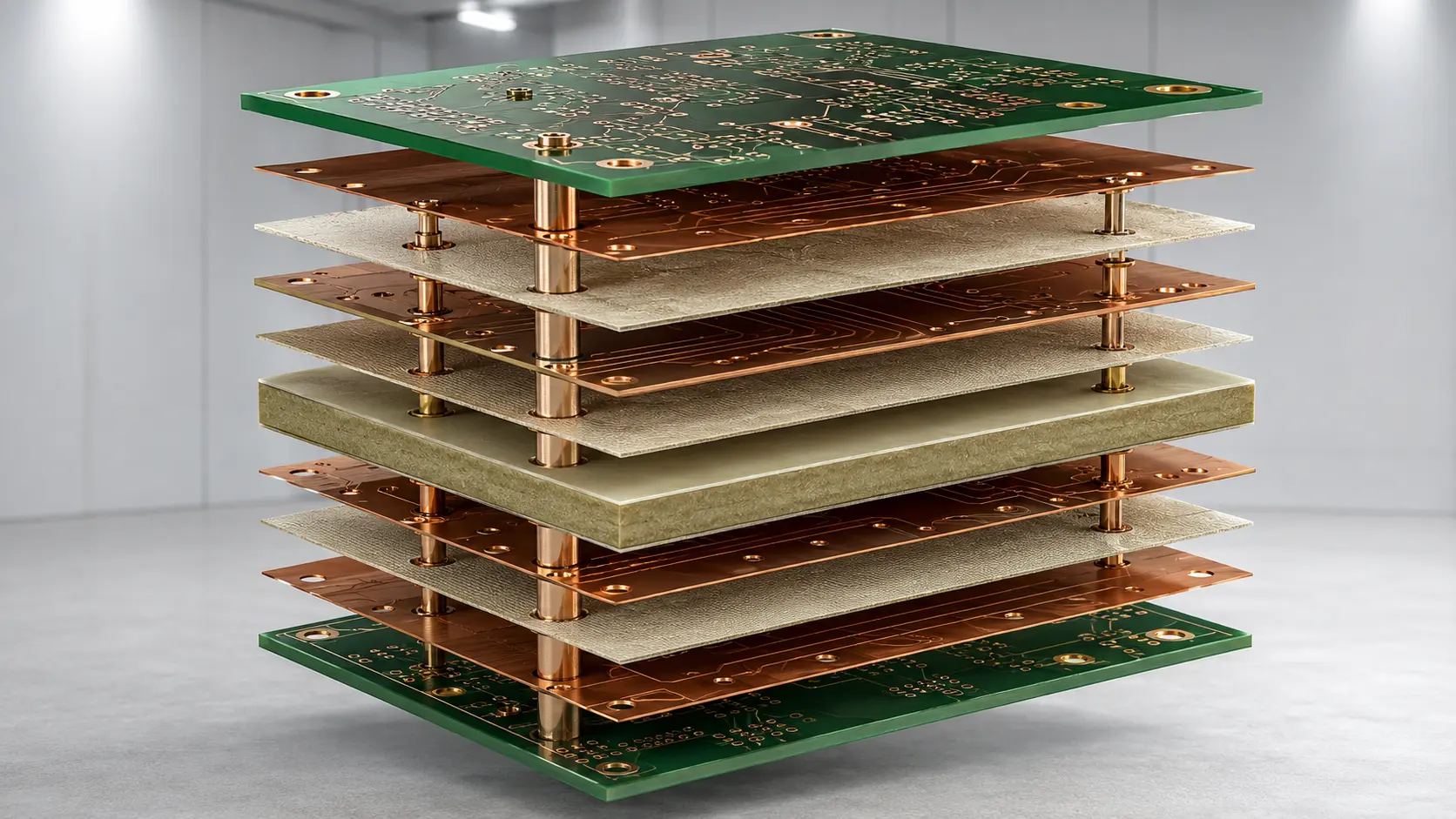
2. Select Materials and Copper Together
Multilayer construction uses copper-clad cores and prepreg bonding layers. The laminate family, glass style, resin content, flow behavior, Tg, electrical properties, and thickness availability affect both performance and manufacturability. The choice should match operating temperature, frequency, mechanical stress, reliability target, and supply availability.
The PCB material selection guide explains why FR4, high-Tg, high-frequency, and thermal materials should not be treated as interchangeable labels. For a multilayer board, mixing material requirements without a qualified construction can create bonding, thickness, and processing risks.
Copper distribution also matters. A layer with large solid planes behaves differently during etching and lamination from a layer containing sparse fine traces. Designers can improve balance by avoiding extreme copper-density differences where possible and by allowing the fabricator to add suitable thieving or balancing features outside functional circuitry.
Common mistake: Fixing the total board thickness while independently changing copper weight, dielectric spacing, and material. These values interact. Any stack-up change should be checked again for thickness, impedance, resin fill, symmetry, and manufacturing availability.
3. Control Inner-Layer Imaging and Registration
Each inner copper layer is imaged and etched before the multilayer set is laminated. The factory must compensate for material movement and align the layers using registration targets and process data. Small errors can reduce annular ring, shift internal clearances, or move a drilled hole closer to an unintended copper feature.
Registration capability depends on board size, layer count, material system, copper distribution, feature density, and process controls. Critical designs should provide sensible pad sizes and clearances rather than relying on ideal mathematical alignment. IPC lists printed-board design standards that can help establish formal design requirements.
4. Manage Lamination, Resin Flow, and Board Symmetry
During lamination, prepared inner layers, prepregs, and outer copper foils are stacked and pressed under controlled heat and pressure. The resin softens, flows, fills spaces around copper features, and cures into the final bonded structure. Press cycle, material condition, copper pattern, panel construction, and storage all influence the result.
Insufficient resin may leave weak fill around heavy copper or dense features. Excessive or uneven flow may affect dielectric thickness. An asymmetric stack-up or unbalanced copper distribution can also contribute to bow and twist. The solution is not a single universal prepreg; it is a reviewed construction matched to the actual pattern.
5. Coordinate Drilling and Plated Via Reliability
After lamination, mechanical or laser drilling creates the holes required by the design. Drilling must account for layer position, material thickness, hole aspect ratio, smear removal, and the finished hole requirement. The subsequent copper deposition and electroplating form the conductive barrel that connects the selected layers.
Through holes, blind vias, buried vias, and microvias have different manufacturing flows and reliability considerations. The PCB via types guide helps compare these structures before the design commits to unnecessary complexity.
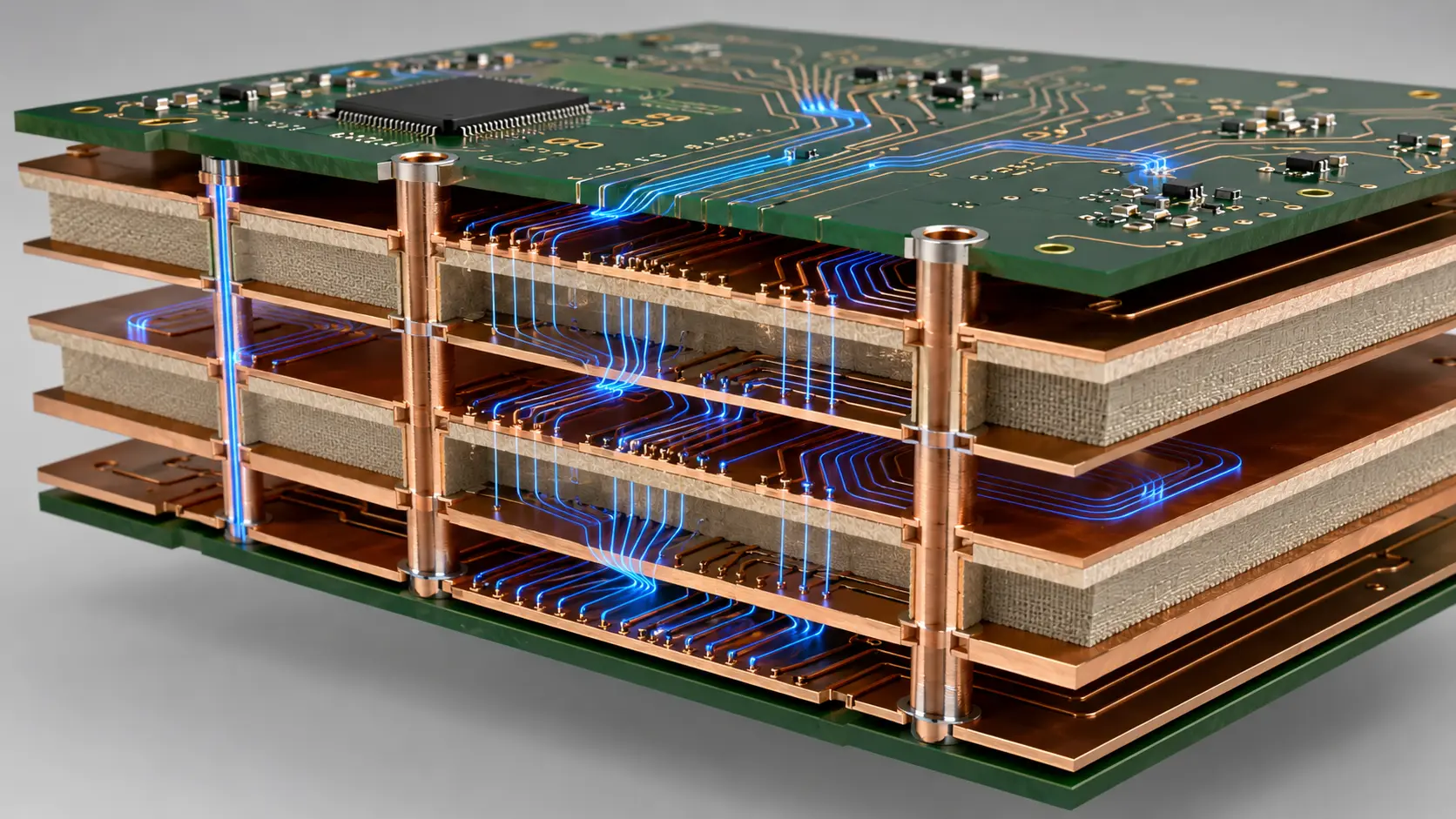
| Manufacturing stage | Potential risk | Useful control |
|---|---|---|
| Inner-layer imaging | Feature shift, over-etch, reduced conductor width | Artwork compensation, AOI, process coupons |
| Lamination | Voids, weak bonding, thickness variation, bow and twist | Qualified material set, controlled press cycle, balanced construction |
| Drilling | Hole offset, smear, rough wall, drill wear | Tool-life control, registration data, desmear process |
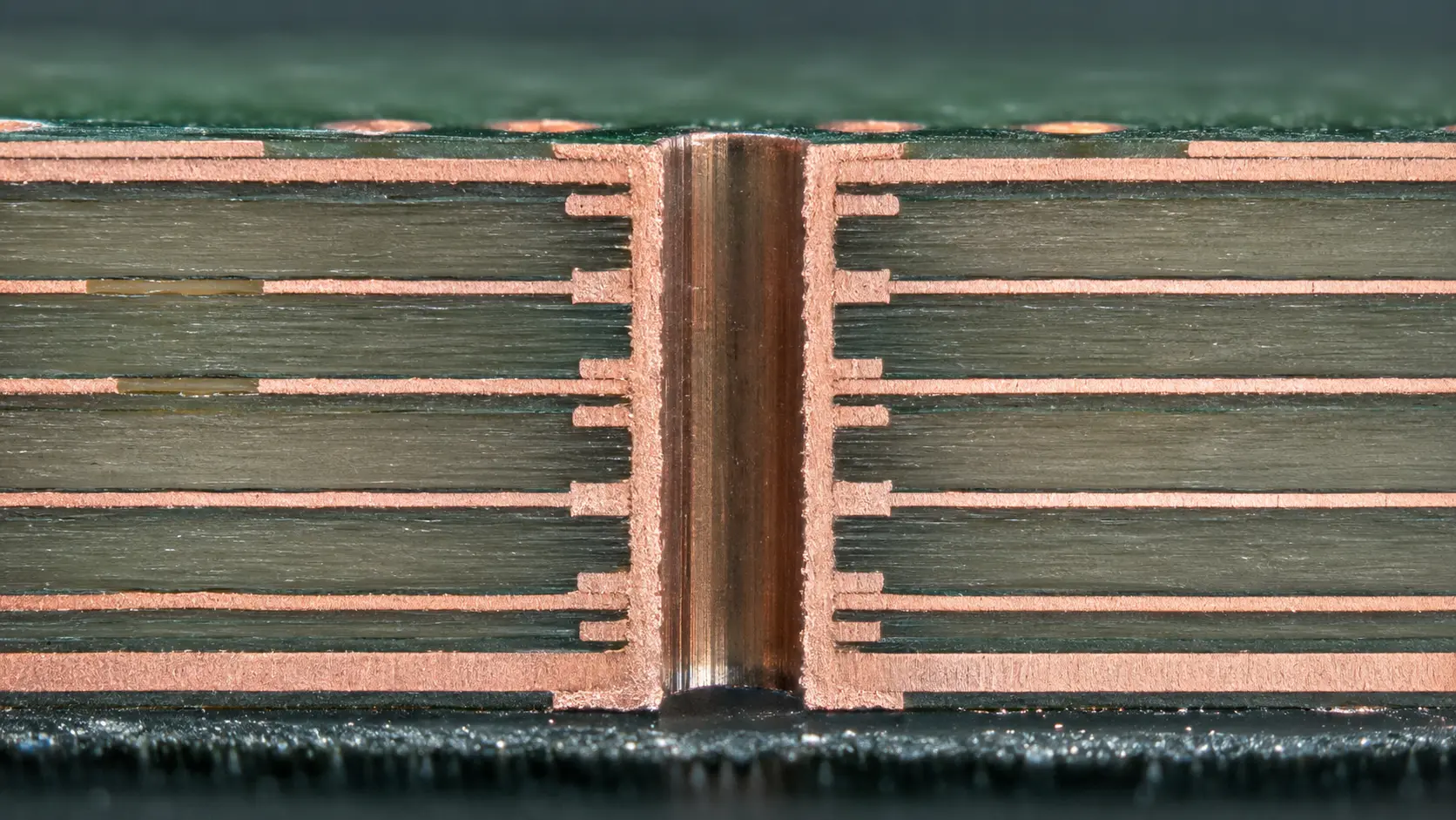
| Hole plating | Thin copper, voids, weak interconnection | Bath control, coupon measurement, microsection review |
| Final inspection | Hidden defects or wrong electrical connection | Electrical test, dimensional check, AOI and specified acceptance criteria |
6. Treat Controlled Impedance as a Construction Requirement
Controlled impedance is determined by the manufactured combination of trace width and thickness, dielectric spacing and properties, reference-plane location, solder mask, and process tolerance. A calculator result based on a generic dielectric value is not enough if the production stack-up uses different materials or thicknesses.
Identify every controlled structure by layer and type, then agree on the production geometry and test method. Our controlled impedance PCB guide explains the information a supplier needs for stack-up modelling and coupon verification.
7. Run DFM Before Releasing the Order
A multilayer DFM review should compare all manufacturing files and identify conflicts in layer names, board outline, drill pairs, via types, copper notes, impedance tables, finished thickness, and tolerances. It should also flag narrow annular rings, copper close to routed edges, problematic slots, unbalanced construction, and features beyond the selected process capability.
The PCB DFM checklist provides a practical pre-order review. For custom stack-ups, contact the PCB fabrication team before routing is completely locked, especially when the design uses tight impedance, blind or buried vias, unusual thickness, heavy copper, or a specific material.
8. Define Inspection and Acceptance Evidence
Multilayer quality cannot be judged only from the outer surface. Useful controls may include inner-layer AOI, electrical testing, dimensional measurement, impedance coupons, bow-and-twist checks, solderability verification, and microsection analysis of plated holes and internal registration. The required evidence should match the product risk and agreed specification.
A documented PCB manufacturing quality control plan gives the buyer and supplier the same acceptance target. IPC information on printed-board performance and acceptability standards can provide a common baseline, with any project-specific additions stated on the order documentation.
Buyer checklist: Before ordering, confirm layer order, material, copper by layer, finished thickness, via structure, impedance requirements, surface finish, tolerances, test method, and acceptance standard. Freeze the approved stack-up with a revision number so an obsolete version cannot enter production.
Final Thoughts
Reliable multilayer PCB manufacturing depends on coordinated data and controlled process transitions. Stack-up design affects material selection, imaging, lamination, drilling, plating, impedance, mechanical dimensions, and inspection. Treating those decisions as one construction reduces avoidable revisions and gives the supplier a clearer path to repeatable production.
EazyPCB supports multilayer PCB fabrication, stack-up review, controlled impedance, prototyping, inspection, and production. To review a custom multilayer project, contact EazyPCB with the layer data, fabrication drawing, drill files, and operating requirements.
