
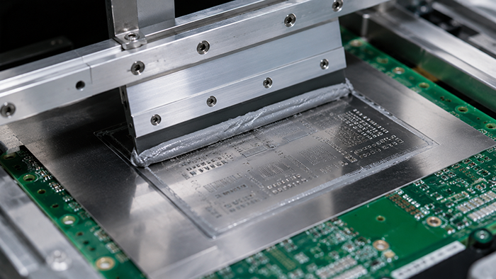
SMT stencil design is one of the most important factors in PCB assembly quality. Before components are placed, solder paste must be printed accurately onto the PCB pads. If paste volume is too much, too little, or uneven, the assembly may suffer from solder bridges, insufficient solder, tombstoning, voids, or weak joints.
For reliable SMT assembly, stencil design should be considered together with PCB pad design, component package type, solder paste, panelization, and reflow profile.
What Is an SMT Stencil?
An SMT stencil is usually a thin stainless steel sheet with laser-cut openings, called apertures. During solder paste printing, the stencil is aligned over the PCB and solder paste is pushed through the apertures onto the pads.
The stencil controls how much paste is deposited on each pad. This means stencil thickness, aperture size, aperture shape, and paste release behavior directly affect solder joint quality.
Why Stencil Design Matters
A PCB layout may be correct, but poor stencil design can still create assembly defects. Fine-pitch ICs, QFN packages, BGAs, small passive components, connectors, and thermal pads all need suitable paste volume.
If your project includes assembly, the production data should include not only Gerber files but also a clear BOM and pick-and-place file. These files help the assembly team understand component packages and placement requirements before stencil review.
Stencil Thickness
Stencil thickness affects the total volume of solder paste. A thicker stencil deposits more paste, while a thinner stencil deposits less. Standard stencil thickness may work for many components, but mixed packages can create challenges.
For example, large connectors may need more paste, while fine-pitch ICs may need less paste to avoid bridging. In some cases, step stencils or local aperture adjustments may be used to balance different component requirements.
Aperture Reduction and Shape
Aperture design controls paste release and solder volume. For fine-pitch pads, apertures may be slightly reduced to avoid excess solder. For thermal pads under QFN or power components, windowpane patterns can reduce voiding and improve paste distribution.
Rounded corners, home-plate shapes, and modified apertures can also help reduce solder defects for small passive components and fine-pitch devices.
Fine-Pitch, BGA, and QFN Packages
Fine-pitch components are sensitive to solder paste volume and alignment. Too much paste can cause bridges, while too little paste can create open joints. BGA and QFN packages also require careful stencil design because many solder joints are hidden after assembly.
For hidden solder joints, inspection becomes important. Our PCB assembly testing and inspection guide explains how AOI, X-ray, ICT, and functional testing help verify PCBA quality.
Panelization and Stencil Printing
Stencil printing is easier when the PCB panel is stable and properly designed. Small boards often need tooling rails, fiducials, and suitable spacing so the panel can move through the printing and assembly process accurately.
If you are preparing a production panel, see our PCB panelization guide for V-score, mouse bites, tooling rails, and SMT handling considerations.
Common SMT Stencil Problems
- Too much paste on fine-pitch pads causing solder bridges.
- Too little paste causing weak or open solder joints.
- Poor paste release from very small apertures.
- Large thermal pads causing solder voids or floating components.
- Panel movement or poor fiducial design affecting print alignment.
- Stencil design not matching the actual component package.
Standards and Process Control
Electronics manufacturing standards help teams communicate quality expectations. The IPC standards family is widely used across PCB fabrication and assembly, and IPC J-STD-001 is commonly associated with soldered electrical and electronic assemblies.
For production projects, stencil design should be reviewed together with solder paste type, reflow profile, component package data, inspection requirements, and acceptance criteria.
Improve PCBA Quality from the First Step
Good SMT assembly starts before pick-and-place. Accurate solder paste printing helps reduce defects and improves yield, especially for fine-pitch, BGA, QFN, and high-density PCB designs.
EazyPCB supports PCB fabrication and SMT assembly for prototypes and production runs. If you need help reviewing stencil design, assembly files, or paste printing requirements, you can contact our engineering team before production.
