
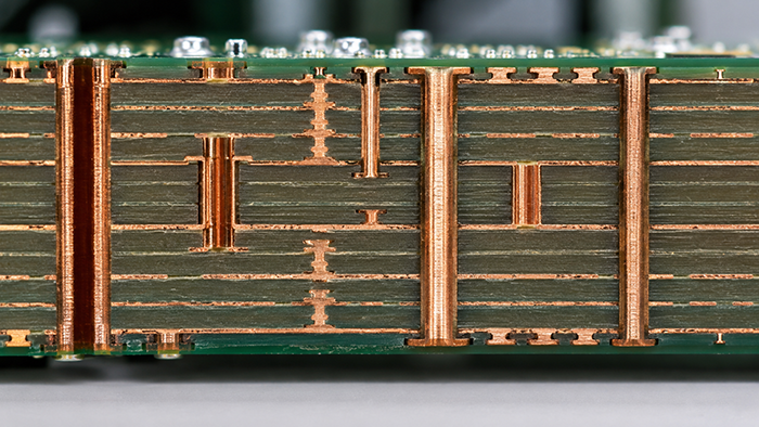
Vias are small plated holes that connect copper layers inside a PCB. They may look simple, but via selection can affect routing density, signal performance, manufacturing cost, assembly reliability, and long-term product quality.
For standard PCB fabrication, through-hole vias are often enough. For dense BGA, high-speed, compact, or multilayer designs, blind vias, buried vias, and microvias may be needed to create a practical layout.
What Is a PCB Via?
A PCB via is a plated connection between layers. In a simple 2-layer PCB, a via connects the top copper layer to the bottom copper layer. In a multilayer PCB, vias can connect different internal and external layers depending on the stack-up and manufacturing process.
The main via parameters include drill diameter, finished hole size, pad diameter, annular ring, plating thickness, aspect ratio, and whether the via is filled, capped, tented, or left open.
1. Through-Hole Via
A through-hole via passes through the entire PCB from the top layer to the bottom layer. It is the most common and usually the most economical via type.
Through-hole vias are suitable for many 2-layer, 4-layer, and standard multilayer boards. They are easy to inspect and widely supported by PCB manufacturers. However, they also take space on every layer they pass through, which may limit routing density in compact designs.
2. Blind Via
A blind via connects an outer layer to one or more inner layers, but it does not pass through the entire board. Because it stops inside the PCB, it can save routing space on other layers.
Blind vias are useful for dense designs, especially under BGA packages and compact consumer electronics. They usually require more advanced fabrication steps, so cost and lead time may be higher than standard through-hole vias.
3. Buried Via
A buried via connects internal layers only and cannot be seen from the outside of the PCB. It is used when inner-layer routing needs connections without occupying space on the top or bottom surface.
Buried vias can help improve routing flexibility in complex multilayer designs, but they increase manufacturing complexity. The PCB stack-up and lamination sequence must be planned carefully before production.
4. Microvia
A microvia is a very small via, usually created by laser drilling. Microvias are common in HDI PCB designs because they allow high-density routing, fine-pitch BGA fanout, and smaller board sizes.
If your design includes microvias, read our HDI PCB and microvia guide. Microvias can improve density, but they need careful stack-up planning, reliability review, and manufacturer confirmation.
Via-in-Pad and Filled Vias
For fine-pitch BGA and compact layouts, vias may be placed directly in component pads. This is called via-in-pad. In many cases, via-in-pad must be filled and capped to avoid solder wicking, voids, and assembly defects.
Via-in-pad can make routing easier, but it adds process requirements. It should be discussed before production, especially when the PCB will go through SMT assembly.
How Via Choice Affects PCB Cost
Through-hole vias are usually the most cost-effective. Blind vias, buried vias, stacked microvias, copper-filled vias, and via-in-pad structures add process steps and may increase cost.
Cost is not only about the via itself. Via choice affects layer count, stack-up, yield, inspection difficulty, and assembly risk. Sometimes using advanced vias can reduce board size or layer count, but sometimes a simpler via structure is more reliable and economical.
Via Selection and Multilayer Stack-Up
Via strategy should be planned together with the PCB stack-up. A 2-layer board, 4-layer board, and high-density multilayer board have very different routing options and constraints.
For more context, see our guide on 2-layer, 4-layer, and multilayer PCB stack-up selection. For high-speed circuits, via stubs and return paths may also affect signal integrity, as discussed in our controlled impedance PCB guide.
DFM Checks for PCB Vias
- Confirm minimum drill size and finished hole size.
- Check annular ring and pad size against manufacturing capability.
- Review aspect ratio for plated through-hole vias.
- Confirm whether vias need tenting, plugging, filling, or capping.
- Check via placement near pads, board edges, and high-current paths.
- Confirm blind, buried, or microvia stack-up with the manufacturer.
Industry design standards such as IPC standards help define common PCB design and manufacturing expectations. The IPC-2221 design standard family is often referenced for printed board design requirements.
Choose the Right Via Before Production
The best via type depends on board density, component pitch, layer count, current requirement, signal speed, cost target, and reliability expectation. A simple through-hole via may be perfect for many boards, while HDI designs may require blind vias or microvias.
EazyPCB supports standard and advanced PCB manufacturing capabilities. If you are unsure whether your via structure is manufacturable, review our PCB DFM checklist or contact our engineering team before production.
