
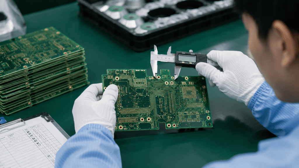
PCB manufacturing tolerances define the acceptable variation between the design file and the finished circuit board. No manufacturing process is perfectly exact, so every PCB has practical limits for board thickness, hole size, outline dimensions, copper width, solder mask, and plating.
Understanding tolerances before PCB fabrication helps avoid assembly problems, enclosure fit issues, high-current risks, and unnecessary production delays. It also helps engineers decide which dimensions are critical and which can follow standard production capability.
Why PCB Tolerances Matter
A PCB can pass electrical testing but still create problems if the mechanical or manufacturing tolerances are not suitable. Mounting holes may not align with the enclosure, connectors may not fit correctly, or copper traces may be too close to the manufacturer’s process limit.
For this reason, tolerance review should be part of the same process as a PCB DFM check. The goal is not to make every feature extremely tight, but to define the right tolerances where they actually matter.
Board Thickness Tolerance
Board thickness affects mechanical fit, connector engagement, impedance, stiffness, and thermal behavior. A nominal 1.6 mm PCB may have a practical thickness tolerance depending on material, copper thickness, layer count, and lamination process.
If the PCB slides into a card edge connector, fits into a tight enclosure, or needs controlled impedance, board thickness should be clearly specified. For standard boards, normal production tolerance is usually acceptable, but mechanical-critical products need extra review.
Hole Size and Drill Tolerance
Finished hole size is affected by drill diameter, plating thickness, and process variation. Plated through holes are usually drilled larger before copper plating so that the final finished hole meets the required size.
For connectors, press-fit pins, mounting holes, and mechanical alignment holes, finished hole tolerance is important. If the project includes different PCB via types, via size, annular ring, and aspect ratio should also be checked before production.
Board Outline and Routing Tolerance
PCB outline tolerance affects whether the board fits into the final product. Routed edges, V-score lines, slots, cutouts, and irregular shapes all have manufacturing limits.
If the board must fit into a plastic enclosure, metal housing, slot, rail, or connector, include clear mechanical drawings. Gerber files alone may not communicate every critical fit requirement. Our Gerber file checklist explains which production files should be reviewed before ordering.
Copper Width, Spacing, and Copper Thickness
Copper traces and spacing also have manufacturing tolerances. Very narrow traces, small gaps, heavy copper, and high-current designs require more careful review than standard signal boards.
Copper thickness affects current capacity, etching behavior, and trace accuracy. If your design uses 2 oz copper or heavy copper, see our PCB copper thickness guide. Thicker copper may require wider trace and spacing rules.
Solder Mask and Silkscreen Tolerance
Solder mask registration has its own tolerance. If the solder mask opening is too close to a pad edge, it may partially cover the pad or expose extra copper. Fine-pitch SMT pads need special attention.
Silkscreen also needs clearance from exposed pads. Text, polarity marks, and reference designators should remain readable without overlapping solderable areas, especially for boards that will go through inspection or manual repair.
When Should You Specify Tight Tolerances?
- When the PCB must fit into a tight enclosure.
- When connectors, card edges, or press-fit parts depend on exact dimensions.
- When controlled impedance depends on stack-up and dielectric thickness.
- When high-current traces, heavy copper, or small spacing are near process limits.
- When mounting holes or slots are used for mechanical alignment.
- When production volume is high and repeatability is critical.
Standards and Quality Control
Standards help align expectations between designers, manufacturers, and assembly teams. The IPC standards family is widely used in PCB manufacturing, and ISO 9001:2015 is a common quality management reference for production suppliers.
For production orders, tolerance requirements should be reviewed together with inspection plans, acceptance criteria, and quality control documentation.
Confirm Critical Tolerances Before Production
The best approach is to mark only the truly critical dimensions as tight tolerances and keep other features within standard manufacturing capability. This helps control cost while protecting product function.
EazyPCB supports prototype and production PCB projects with engineering review and PCB manufacturing capabilities. If your design has critical board thickness, hole size, outline, copper, or assembly tolerance requirements, you can contact our engineering team before production.
“`