
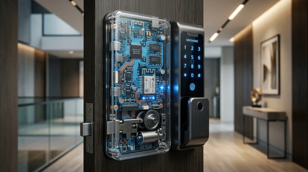
The Role of PCBA in Smart Lock Connectivity
Wireless Protocols: Wi-Fi, Bluetooth, and Zigbee
The connectivity of modern smart locks is fundamentally dependent on the Printed Circuit Board Assembly (PCBA) and its ability to integrate various wireless communication protocols. Wi-Fi, Bluetooth Low Energy (BLE), and Zigbee are the most common standards utilized in today’s smart home ecosystems. Wi-Fi provides a direct connection to the internet, allowing for remote access from anywhere in the world. However, it is also a significant consumer of power, which is a critical consideration for battery-operated devices. Bluetooth Low Energy, on the other hand, offers a more power-efficient solution for local connectivity, enabling users to unlock their doors using their smartphones as they approach. Zigbee and Z-Wave are often used in mesh networks, providing reliable communication between devices and a central hub. The PCBA must be designed to handle these different frequencies and protocols without interference, ensuring a seamless user experience. Engineers must carefully select the radio frequency (RF) components and antenna designs to maximize range and stability. Proper shielding and ground plane optimization on the PCB are essential to prevent noise from the digital circuits from affecting the sensitive wireless signals.
Moreover, the integration of multiple protocols on a single PCBA is becoming increasingly common. Dual-mode chips that support both Wi-Fi and BLE allow for the best of both worlds: high-speed remote access and low-power local control. This complexity requires advanced PCB layout techniques, such as multi-layer designs and controlled impedance routing, to maintain signal integrity across the entire board. The placement of components is also crucial; for instance, keeping the power-hungry Wi-Fi module away from the sensitive analog circuits helps in reducing noise. As the demand for smarter and more connected homes grows, the role of PCBA in managing these diverse communication channels becomes even more vital.
Integrating Secure MCUs for Robust Communication
At the heart of every smart lock PCBA is a Microcontroller Unit (MCU) that manages all functions, from processing sensor data to controlling the locking mechanism and handling wireless communication. For smart locks, security-focused MCUs are a necessity rather than a luxury. These specialized processors include hardware-based security features such as True Random Number Generators (TRNGs), Secure Boot, and cryptographic accelerators. These features ensure that the firmware running on the lock has not been tampered with and that all data being transmitted is encrypted using robust algorithms. The MCU also acts as a gatekeeper for the wireless modules, ensuring that only authorized commands are executed. Integrating these secure MCUs requires deep knowledge of both hardware design and software development, as the PCBA must provide a stable environment for the MCU to function correctly under various conditions.
The choice of MCU also affects the overall power profile of the smart lock. High-performance MCUs with advanced sleep modes allow the lock to remain in a low-power state for the majority of the time, waking up only when a sensor is triggered or a wireless signal is received. This intelligent power management is key to achieving long battery life. Furthermore, the PCBA design must account for the specific requirements of the MCU, such as precise voltage regulation and decoupling capacitors to filter out high-frequency noise. By selecting the right MCU and designing the PCBA around its strengths, manufacturers can create smart locks that are not only highly secure but also incredibly reliable and efficient.
Securing Data Transmission via Advanced PCBA Design
Encryption Modules and Hardware Security Keys
One of the most significant security threats to smart locks is the interception of data transmitted over the air. To combat this, advanced PCBA designs incorporate dedicated encryption modules and hardware security keys. These components are designed to perform complex mathematical operations required for encryption and decryption far more efficiently and securely than a general-purpose processor. By storing cryptographic keys in a secure, tamper-resistant area of the chip (often referred to as a “Secure Element”), the PCBA ensures that even if a hacker gains physical access to the device, they cannot easily extract the keys. This hardware-level security is a cornerstone of modern smart lock architecture, providing a level of protection that software-based solutions simply cannot match.
The use of asymmetric encryption, such as Elliptic Curve Cryptography (ECC), is becoming the standard for securing communication between the smart lock and the user’s smartphone. This involves a public-private key pair where the private key never leaves the secure module on the PCB. The PCBA must be designed to facilitate the high-speed data transfer required for these encryption processes without introducing delays or increasing power consumption significantly. This often involves using dedicated buses for communication between the MCU and the security chip. As cyber threats become more sophisticated, the inclusion of these advanced security components on the PCBA is essential for maintaining consumer trust in smart home technology.
Minimizing Signal Interference for Reliable Access
Reliability is just as important as security when it comes to smart locks. A lock that fails to open because of signal interference is more than just an inconvenience; it can be a safety hazard. PCBA designers use several techniques to minimize electromagnetic interference (EMI) and ensure reliable connectivity. This includes the use of differential signaling for high-speed data lines, which helps to cancel out noise, and the implementation of robust ground planes to provide a stable reference voltage for all components. Additionally, the use of ferrites and bypass capacitors can help to filter out unwanted high-frequency signals that might interfere with the lock’s wireless modules. The physical layout of the PCB is also optimized to keep high-speed digital lines away from sensitive analog signals and the RF antenna.
Environmental factors also play a role in signal reliability. Smart locks are often installed on metal doors, which can act as a shield and interfere with wireless signals. To overcome this, PCBA designs may include external antenna connectors or use specialized antenna designs that can project signals through or around the metal door. Testing for EMI and electromagnetic compatibility (EMC) is a critical part of the PCBA development process, ensuring that the smart lock meets international standards and functions reliably in the diverse environments of modern homes. By focusing on noise reduction and signal integrity, PCBA connectivity ensures that the smart lock remains a dependable part of the home security system.
Power Management and Reliability in Connected PCBs
Low-Power Consumption Strategies for Battery Longevity
Since most smart locks are powered by standard AA or lithium batteries, maximizing battery life is a top priority for PCBA designers. This is achieved through a combination of hardware and software strategies. On the hardware side, the use of ultra-low-power components, such as voltage regulators with low quiescent current and sensors that consume minimal power in standby mode, is essential. The PCBA layout is also designed to minimize parasitic resistance and capacitance, which can lead to unnecessary power loss. Software-wise, the MCU is programmed to keep most of the lock’s systems in a deep-sleep state, only waking them up when absolutely necessary. This “wake-on-event” architecture is highly effective at conserving energy while still providing responsive performance when needed.
Another important aspect of power management is the ability of the PCBA to accurately monitor battery levels. This allows the lock to provide users with timely warnings when the batteries are running low, preventing unexpected lockouts. Some advanced PCBA designs even include energy harvesting capabilities, such as small solar panels or kinetic energy modules, to supplement the main battery power. As the number of connected devices in the home continues to grow, the pressure on battery life will only increase, making innovative power management on the PCBA more critical than ever. A well-optimized PCBA can mean the difference between a smart lock that requires battery changes every few months and one that lasts for over a year.
Redundancy Circuits to Prevent Lockouts
To ensure that users are never locked out of their homes due to a technical failure, PCBA designs often include redundancy circuits and fail-safe mechanisms. This might include a secondary MCU that can take over basic functions if the main processor fails, or redundant power paths that ensure the lock remains functional even if a component in the primary power circuit fails. Some smart locks also include a physical override, such as a traditional keyway or an external battery terminal that can provide temporary power if the internal batteries are completely dead. The PCBA must be designed to integrate these backup systems seamlessly, ensuring that they do not interfere with the lock’s normal operation but are ready to activate at a moment’s notice.
Thermal management is another factor in PCBA reliability. Smart locks are exposed to a wide range of temperatures, from freezing winters to scorching summers. The components selected for the PCBA must be rated for industrial temperature ranges to ensure they do not fail under extreme conditions. Furthermore, the PCB layout must account for thermal expansion and contraction, which can stress solder joints and lead to intermittent connections over time. By incorporating redundancy and focusing on environmental robustness, PCBA connectivity provides the reliability that homeowners expect from a high-quality smart lock. These design considerations are essential for creating a product that is not just smart, but also durable and trustworthy.
Over-the-Air (OTA) Updates and Firmware Security
Ensuring Seamless and Secure Remote Updates
One of the greatest advantages of connected smart locks is the ability to receive Over-the-Air (OTA) firmware updates. These updates allow manufacturers to continuously improve the security and functionality of the lock after it has been installed. The PCBA plays a crucial role in this process by providing the necessary connectivity and memory to handle the update. A typical OTA process involves downloading the new firmware in the background, verifying its integrity and authenticity, and then applying the update during a period of inactivity. To ensure that the process is seamless, the PCBA often includes extra flash memory to store the new firmware image alongside the currently running version. This “A/B” update strategy allows for a quick rollback if something goes wrong during the update process.
Security is the most critical part of the OTA process. If a hacker could deliver a malicious firmware update, they could gain complete control over the lock. To prevent this, the PCBA connectivity must be secured using end-to-end encryption and digital signatures. The secure MCU on the PCB verifies the signature of the new firmware using a public key stored in its secure area before allowing the update to proceed. This ensures that only authorized updates from the manufacturer can be installed. By enabling secure and seamless OTA updates, PCBA connectivity ensures that the smart lock remains protected against the latest security threats throughout its entire lifespan.
Rollback Mechanisms and Tamper Protection
In addition to secure updates, modern smart lock PCBAs are equipped with rollback mechanisms and tamper protection features. A rollback mechanism ensures that if a firmware update fails or causes an error, the lock can automatically return to the previous stable version. This prevents the lock from becoming “bricked” and unusable. Tamper protection, on the other hand, is designed to detect physical attempts to compromise the lock. This might include sensors on the PCB that detect when the case has been opened or when excessive force has been applied. If tampering is detected, the lock can respond by disabling certain functions, sounding an alarm, or sending an immediate notification to the user’s smartphone.
These features are integrated directly into the PCBA design, requiring specialized circuitry and careful programming. For example, tamper-evident switches must be positioned in a way that they cannot be easily bypassed, and the MCU must be programmed to handle tamper events as high-priority interruptions. The use of potting compounds or conformal coatings on the PCB can also provide an additional layer of protection against physical tampering and environmental damage. These advanced security measures, combined with the power of PCBA connectivity, make modern smart locks one of the most secure components of the modern smart home. As the technology continues to mature, we can expect even more sophisticated protection features to be integrated into the PCBA.
Future Trends: Matter Protocol and Next-Gen Connectivity
The Shift Towards Unified Smart Home Standards
The future of smart lock connectivity is being shaped by the move towards unified industry standards, with the Matter protocol at the forefront. Matter is an open-standard connectivity protocol designed to ensure that smart home devices from different manufacturers can work together seamlessly and securely. For smart lock PCBA designers, this means moving away from proprietary protocols and towards a more standardized architecture. Matter-compatible PCBAs will likely use Thread, a low-power mesh networking protocol, for local communication, and Wi-Fi for high-bandwidth tasks. This shift will simplify the design process and allow for greater interoperability, making it easier for consumers to build a truly integrated smart home.
Implementing the Matter protocol on a smart lock PCBA requires a significant amount of processing power and memory, as well as support for the latest security standards. This will drive the adoption of more powerful and efficient MCUs and specialized communication chips. The PCBA must also be designed to handle the complex networking requirements of Matter, including support for IPv6 and advanced device discovery mechanisms. As more and more manufacturers adopt Matter, we will see a new generation of smart locks that are not only more secure and reliable but also much easier to use. PCBA connectivity will continue to be the key enabler of this unified and secure smart home future.
Biometric Integration and Edge AI on the PCB
Another exciting trend in smart lock technology is the integration of biometric sensors and edge AI directly onto the PCBA. Biometric features, such as fingerprint scanners and facial recognition modules, provide a highly secure and convenient way to unlock doors. These sensors generate large amounts of data that must be processed quickly and securely. By using edge AI—AI processing that takes place on the device itself rather than in the cloud—the PCBA can recognize a user’s biometrics in milliseconds while keeping their sensitive data local and secure. This requires high-performance processors with dedicated AI accelerators to be integrated into the PCBA design.
The inclusion of edge AI also allows for more intelligent features, such as the ability to detect unusual patterns of behavior or to recognize specific sounds, like a window breaking. These features can be used to trigger alerts and provide an even higher level of security for the home. Designing a PCBA that can handle these advanced tasks while remaining power-efficient and cost-effective is a major challenge for engineers. However, the benefits in terms of security and user experience are significant. As PCBA technology continues to advance, we will see even more innovative features being integrated into the next generation of smart locks, further securing the modern smart home. The journey of PCBA connectivity in smart locks is only just beginning, and the future looks incredibly bright.
