
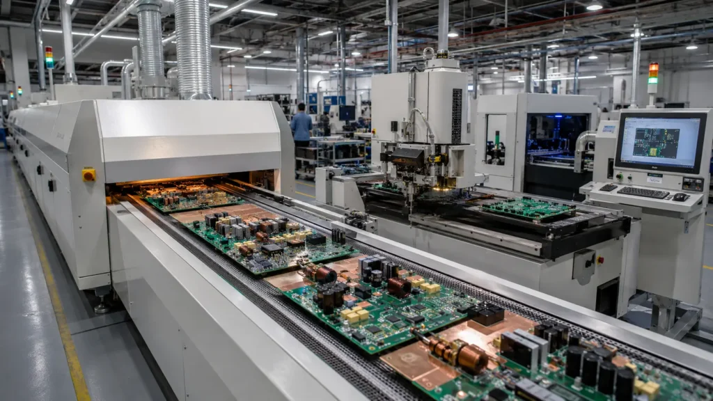
Power supplies, motor controllers, charging systems, LED drivers, industrial converters, battery products, and energy equipment all place special demands on printed circuit boards. These products may carry higher current, switch significant power, generate concentrated heat, and use components with large thermal pads or heavy terminals. As a result, PCB manufacturing for power electronics must connect electrical design, board construction, thermal management, assembly, and testing from the beginning.
A thicker copper specification alone does not make a power PCB reliable. Current must have a complete path through traces, planes, vias, solder joints, connectors, and cables. Heat must also move from the component junction through the package, PCB, thermal interface, heat sink, and enclosure. A weakness anywhere in that chain can limit the finished product.
Engineering principle: Specify current, voltage, duty cycle, ambient temperature, cooling conditions, and acceptable temperature rise before selecting copper thickness or board material. Without the operating conditions, the PCB supplier can manufacture the drawing but cannot validate the design intent.
1. Define the Electrical and Thermal Load First
Start with the worst realistic operating condition rather than only the nominal rating. Continuous current, peak current, switching frequency, startup events, duty cycle, airflow, enclosure temperature, and nearby heat sources all influence the board. The same trace may behave differently in open air, inside a sealed housing, or next to a hot transformer.
It is also useful to review the complete PCB manufacturing process before releasing files. Fabrication notes, stack-up, copper requirements, drill data, surface finish, assembly files, and test requirements should describe the same product instead of conflicting with one another.
| Design concern | Why it matters | Information for manufacturing review |
|---|---|---|
| Current path | Affects voltage drop and conductor heating | Continuous and peak current, trace geometry, plane transitions, via count |
| Voltage spacing | Influences electrical isolation and safety | Working voltage, environment, insulation needs, applicable product standard |
| Heat generation | Changes component life and output stability | Loss estimate, heat-source locations, airflow, heat sink and enclosure contact |
| Power components | Large pads and terminals affect soldering | Package drawings, thermal-pad design, polarity, special assembly instructions |
| Verification | Visual inspection alone cannot prove load performance | Electrical limits, functional procedure, test points, load and temperature criteria |
2. Choose Copper and Board Construction as a System
Copper weight, finished conductor thickness, trace width, spacing, layer count, and via structure must work together. Increasing copper may improve current capacity, but it can also affect etching tolerances, minimum spacing, hole plating, resin filling, finished thickness, and assembly thermal balance.
Our PCB copper thickness guide explains the manufacturing trade-offs in more detail. Trace geometry should also be reviewed using the actual application conditions; the trace width and current capacity guide provides a practical starting point. IPC publishes board design standards that can support formal design requirements, but the project still needs its own electrical and thermal validation.
| Construction approach | Useful strength | Important limitation | Typical project fit |
|---|---|---|---|
| Standard multilayer FR4 | Combines control, signal, and moderate power routing | Thermal path and conductor geometry require careful design | Controllers, converters, mixed-signal power products |
| Heavy-copper FR4 | Supports robust power paths and current distribution | Finer geometry and fabrication options may be restricted | Power distribution, motor and battery applications |
| Metal-core PCB | Provides a direct path toward a metal base | Layer structure and electrical isolation options differ from FR4 | LED, thermal modules, selected power assemblies |
| Separate power and control boards | Allows each board to use a suitable construction | Adds connectors, mechanical interfaces, and assembly steps | Modular systems with distinct power and logic sections |
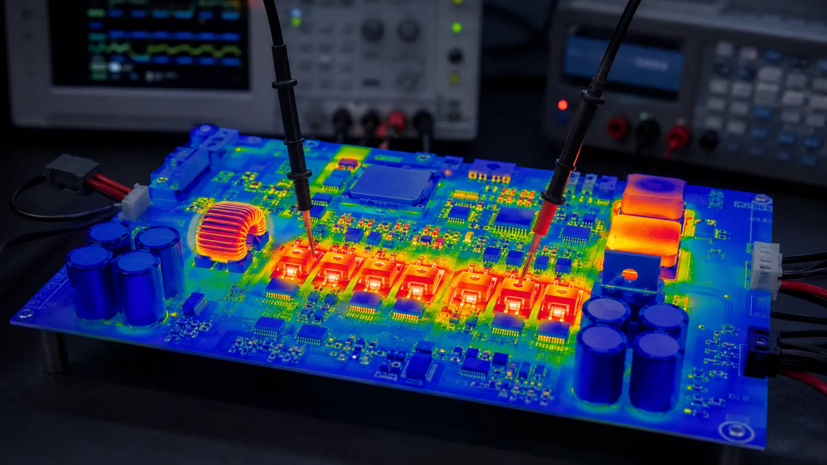
Common mistake: Writing “heavy copper required” without defining the layers, finished copper expectation, minimum geometry, current path, and inspection requirement. Ambiguous notes create quotation differences and can lead to a board that is manufacturable but not suitable for the intended load.
3. Design the Entire Current Path
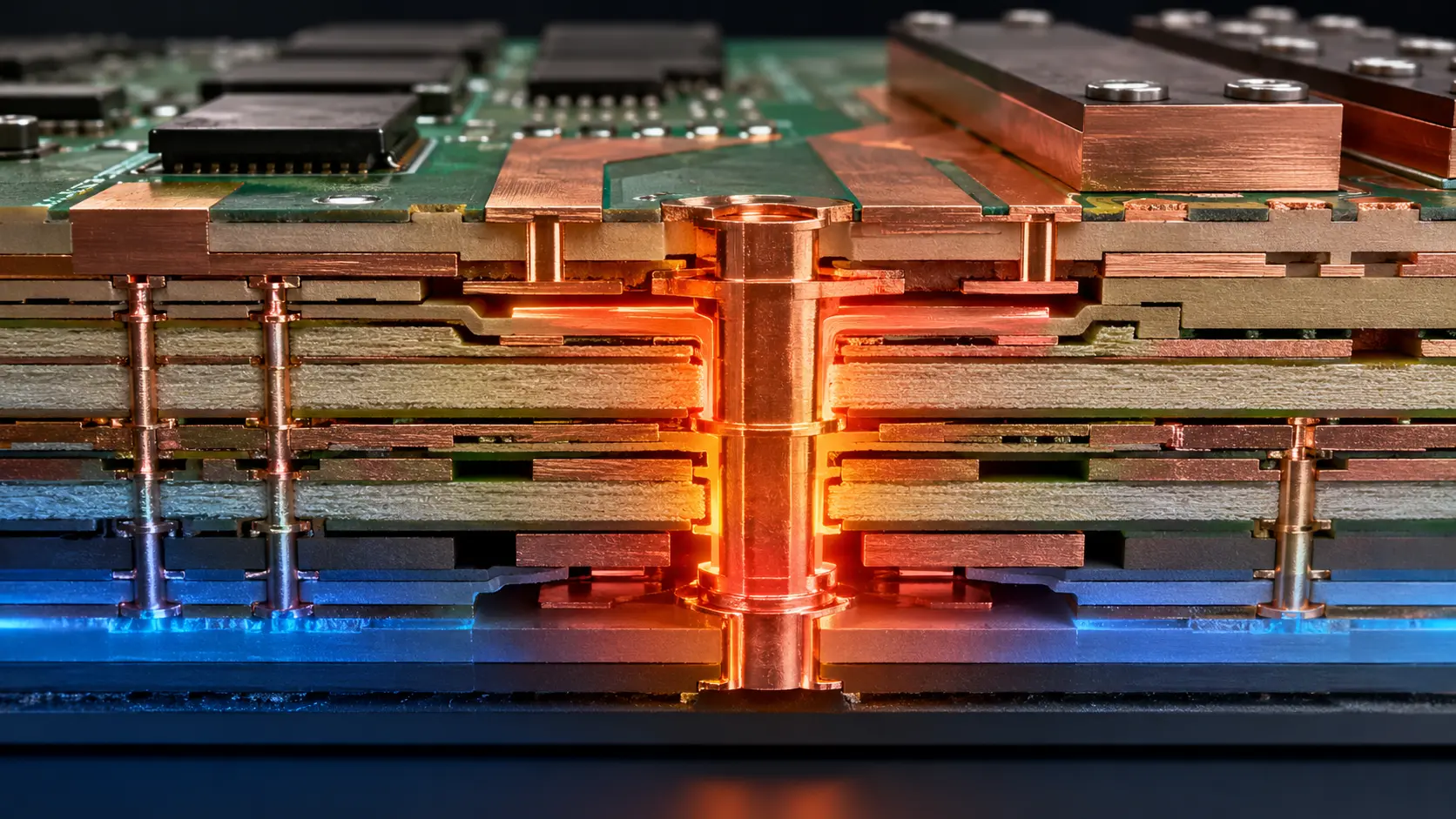
High-current design is not limited to one wide trace. Neck-down areas near pads, layer changes, via arrays, connector pins, fuses, shunts, solder joints, and cable terminals may become the real bottleneck. Copper pours should not be interrupted by unnecessary slots or narrow thermal connections where current must flow.
When current changes layers, via diameter, plating, count, distribution, and thermal interaction all matter. A dense cluster of vias may also affect solder paste or draw solder away from an exposed pad if the assembly design is not coordinated. Early review with the PCB fabrication team helps align electrical intent with practical drill, plating, spacing, and stack-up capabilities.
4. Build a Complete Thermal Path
Thermal management should trace heat from its source to the surrounding environment. Copper planes and thermal vias can spread heat, but they do not remove it unless there is a path to a heat sink, chassis, airflow, or radiating surface. Interface material thickness, screw pressure, enclosure flatness, component height, and airflow direction can change the final result.
Material choice also matters. Standard FR4, high-Tg laminates, metal-core constructions, and specialized materials solve different problems. Review the PCB material selection guide before selecting a premium material only by name. The correct choice depends on temperature, insulation, mechanical design, frequency, fabrication needs, and cost.
5. Plan Assembly for Large Thermal Masses
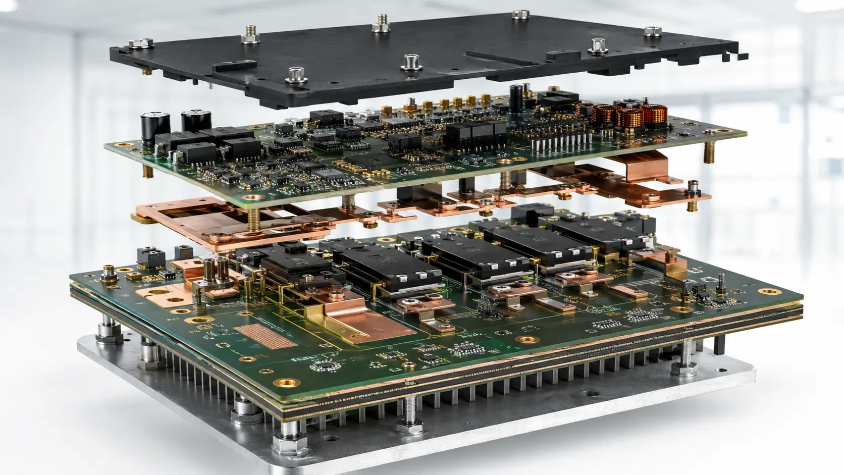
Power PCBAs may include MOSFETs, power packages, inductors, transformers, relays, large capacitors, terminal blocks, busbars, and heat sinks. Large copper areas can draw heat away from solder joints, while mixed component sizes can make one thermal profile difficult for the entire assembly.
For SMT assembly, stencil design, paste coverage on exposed thermal pads, component coplanarity, reflow profile, bottom-side support, and inspection method should be reviewed together. Through-hole power terminals may require wave soldering, selective soldering, or a controlled manual process depending on the design and quantity.
Assembly note: A solder joint can look acceptable from above while hidden thermal-pad coverage, voiding, insufficient barrel fill, or mechanical stress remains unknown. Define which joints need X-ray, cross-section, pull testing, thermal inspection, or other project-specific verification.
6. Test the Board Under Relevant Load
Bare-board electrical testing verifies connectivity and isolation according to the supplied data, but it does not prove that the assembled product will control temperature or carry the intended load. Power PCBA validation may include controlled startup, no-load and full-load behavior, voltage drop, current measurement, thermal stabilization, protection response, switching behavior, and repeated operating cycles.
A clear PCB manufacturing quality control plan should define acceptance criteria before production. IPC information on printed-board acceptance and performance standards can help buyer and supplier establish a common baseline. A quality system such as ISO 9001:2015 supports controlled processes, but product-specific requirements and test evidence are still necessary.
7. Prepare a Complete Manufacturing Package
A useful quotation package should include Gerber or ODB++ data, drill files, stack-up, finished copper requirements by layer, board thickness, material, surface finish, drawing, BOM, pick-and-place file, assembly drawings, polarity notes, programming requirements, and test instructions. Mark critical power nets, heat-generating components, controlled spacing, and mechanically sensitive interfaces.
For custom or high-risk designs, share the expected operating conditions and arrange an engineering review before the order is released. This allows the supplier to identify unclear copper notes, difficult spacing, thermal-pad concerns, component sourcing risks, and test-fixture needs while changes are still inexpensive.
Final Thoughts
Reliable power electronics PCB manufacturing is achieved by coordinating conductor design, material and stack-up, heat flow, component assembly, inspection, and load validation. No single copper weight or laminate can replace that system-level work.
EazyPCB supports PCB fabrication, component sourcing, SMT assembly, prototyping, and production for power and industrial electronics. To review your board construction, BOM, assembly, and test requirements, contact EazyPCB with your design files and operating conditions.
“`