
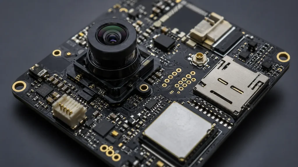
IoT products are getting smaller, smarter, and more connected. Pet feeders, smart cameras, sensors, controllers, wearable devices, gateways, and home automation products all need compact circuit boards that combine communication, power management, control logic, connectors, and sometimes camera or sensor modules. This makes PCB manufacturing for IoT devices more demanding than a simple bare board order.
A reliable IoT PCBA depends on early design planning, stable fabrication, accurate SMT assembly, component availability, and practical testing. If these details are not considered before production, small layout issues can become wireless instability, power problems, assembly defects, or field failures.
Why IoT PCB Manufacturing Needs Careful Planning
IoT boards often combine digital circuits, RF areas, sensors, battery input, connectors, memory, camera modules, and mechanical enclosure constraints. The design must fit the product shape while still leaving enough room for manufacturing tolerances, test points, antenna clearance, and assembly handling.
Before starting an IoT project, it is useful to understand the full PCB manufacturing process. This helps the design team prepare files, stack-up notes, BOM data, pick-and-place files, and test requirements before the order becomes urgent.
1. Match the PCB Layout to the Product Enclosure
Many IoT products have tight mechanical space. A smart pet feeder camera board, for example, may need a lens opening, TF card slot, connector area, mounting holes, and cable routing inside a compact shell. Board shape, connector direction, camera position, and screw holes should be confirmed early.
For custom connected devices, EazyPCB can support PCB fabrication based on special board outlines, mounting requirements, and production files. If the enclosure is already fixed, the PCB should be reviewed together with the mechanical structure instead of separately.
2. Keep Wireless and Antenna Areas Clean
Wireless performance is one of the most common risk points in IoT PCB manufacturing. Wi-Fi, Bluetooth, BLE, cellular, LoRa, and other wireless modules may need clear antenna zones, controlled ground areas, proper keep-out space, and careful component placement.
If a module supplier provides layout recommendations, they should be followed closely. Even when the wireless module is pre-certified, poor antenna clearance, metal enclosure interference, or noisy power routing can still affect real product performance.
3. Prepare BOM and Component Alternatives
IoT PCB projects often depend on wireless modules, camera sensors, connectors, memory devices, power ICs, microphones, motors, or LEDs. A single unavailable component can delay the whole build.
Before SMT assembly, prepare the BOM, approved alternatives, package information, polarity notes, and special assembly instructions. This is especially important for small batch orders where one missing component can stop the entire production run.
4. Design for Programming and Testing
IoT PCBA production should include a practical test plan. Test pads, programming connectors, UART/SWD/JTAG access, power test points, and functional test procedures should be considered before the layout is finalized.
A clear PCB manufacturing quality control plan can include AOI, electrical test, visual inspection, solder joint review, programming checks, and functional testing. For bare board acceptance, references such as IPC standards and IPC-A-600 can help define quality expectations.
5. Use Prototypes to Verify Real Product Behavior
IoT prototypes should test more than basic circuit function. They should verify wireless range, camera image stability, connector fit, charging behavior, power consumption, firmware update flow, heat, and enclosure assembly.
Starting with PCB prototyping helps find design issues before larger orders. When the prototype works well, a controlled low-volume run can be used to verify repeatability and assembly yield.
6. Move Carefully From Prototype to Small Batch
For IoT products, the move from a working prototype to a small batch is a critical step. The team should freeze important parameters such as PCB material, surface finish, copper thickness, connector model, module selection, panelization, test method, and packaging.
The low-volume PCB manufacturing stage is useful for pilot production, market testing, early customer shipments, and design validation before larger production quantities.
7. Link Product Requirements With Manufacturing Decisions
Different IoT products need different PCBA priorities. A battery-powered sensor may focus on low power consumption. A camera device may need stable image module assembly. A smart home controller may require reliable connectors. A pet feeder board may need camera monitoring, TF card storage, motor control, and compact mechanical fit.
For a practical example, see the Smart Pet Feeder Camera PCBA Board. It shows how a compact IoT product can combine a camera module, TF card area, connectors, SMT assembly, and customized board shape.
Final Thoughts
IoT device PCB manufacturing is not only about making a small board. It is about building a stable connected product platform that can be assembled, tested, programmed, and repeated in production.
EazyPCB supports PCB fabrication, SMT assembly, prototyping, small batch production, and PCBA project review for smart devices and connected electronics. If you are developing an IoT product, you can contact us to review your PCB and PCBA requirements.
“`