
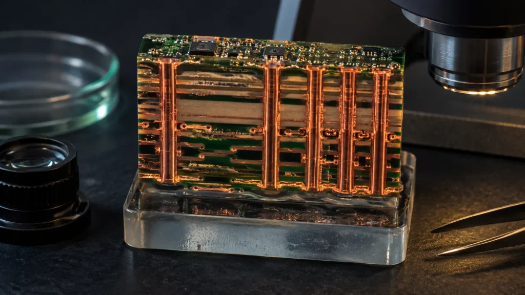
A polished PCB cross-section can make an internal problem visible in a way that electrical test data or an exterior photograph cannot. It may show the copper barrel of a plated hole, an inner-layer connection, a microvia interface, dielectric spacing, resin condition, or a separation hidden inside the board.
But a convincing microscope image is not automatically proof that an entire production lot is acceptable. It represents a selected sample, a selected location, and a selected cutting plane after destructive preparation. Useful PCB manufacturing evidence therefore depends on three things: the right specimen, a controlled preparation method, and acceptance criteria agreed before inspection.
Start with the question: Are you verifying routine lot acceptance, investigating a failure, qualifying a process, or checking a special structure? The same photograph cannot answer all four questions unless the sampling and evaluation plan was designed for that purpose.
1. A Microsection Is a Destructive View Through One Plane
Microsection analysis begins by removing a coupon or board area, mounting it in a suitable material, grinding toward the target feature, polishing the surface, and examining the exposed structure under magnification. IPC lists IPC-TM-650 Method 2.1.1F for manual and semi- or automatic microsectioning. The method covers specimen preparation, mounting, alignment, grinding, polishing, and evaluation considerations.
The cutting direction matters. An axial section through a plated hole can reveal one set of relationships; a transverse section can reveal another. A cut that misses the feature center may make wall thickness, annular geometry, or interface shape look different. For a localized field failure, the correct plane may be determined by X-ray, electrical mapping, microscopy, or other nondestructive evidence before the sample is cut.
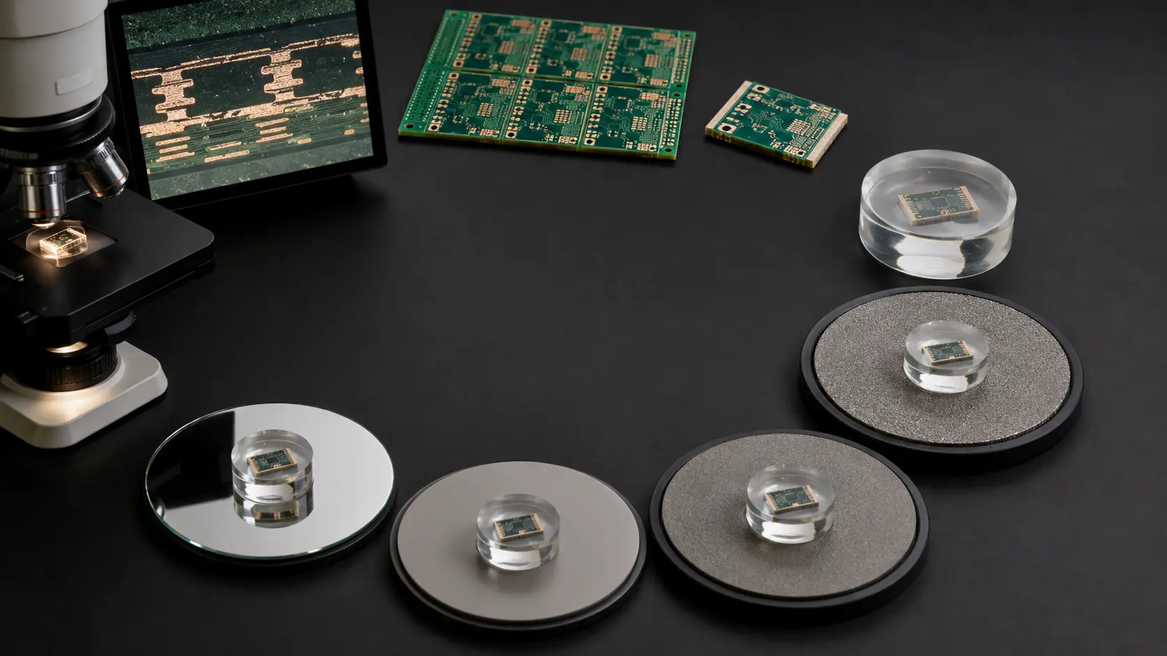
Preparation warning: Smearing, edge rounding, pull-out, scratches, excessive etching, heat, or an off-center grind can create artifacts or hide a real condition. A report should distinguish a product feature from damage introduced during preparation.
2. Define the Evidence Before Selecting the Sample
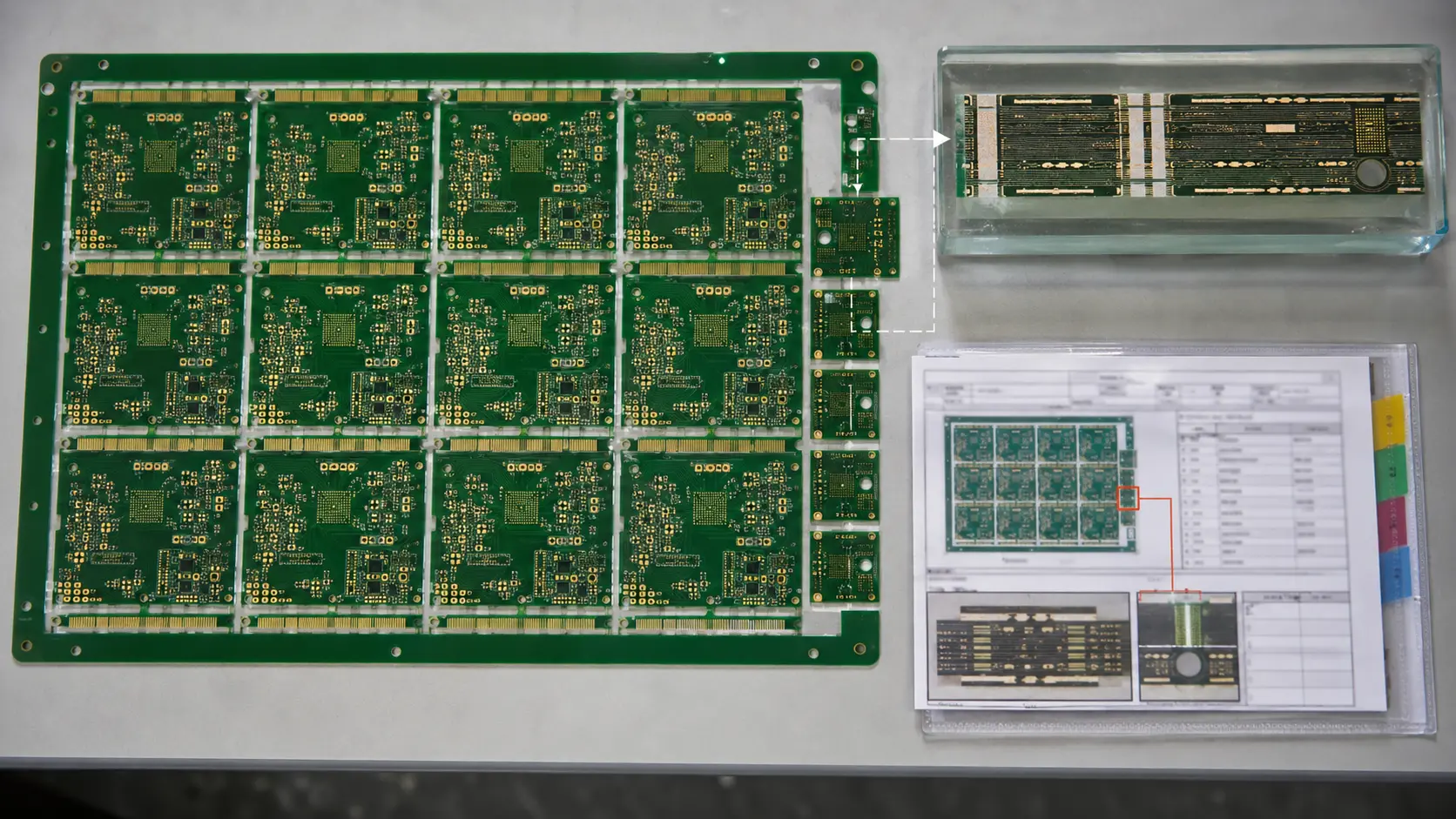
For routine acceptance, a test coupon can provide a controlled representation of selected panel processes. IPC publishes resources for commonly used AB, AB/R, and D coupon designs, including structures for through, blind, buried, and stacked or staggered microvias. The coupon still needs to match the applicable specification, panel, construction, and procurement requirements.
A coupon is not a magical substitute for the product. If the concern involves a connector hole, a local copper imbalance, a buried feature not represented in the coupon, or damage found at a particular board location, a production-board section may be more informative. Conversely, cutting a random good-looking board after a failure may destroy valuable evidence without testing the suspected location.
| Inspection purpose | Possible specimen | Question that must be answered |
|---|---|---|
| Routine lot acceptance | Specified panel coupon | Does the coupon represent the product construction and required processes? |
| First article approval | Coupon plus selected product features | Which design-specific interfaces need evidence before volume production? |
| Failure analysis | Located failed area and comparison sample | Was the physical failure site preserved and identified before cutting? |
| Process qualification | Defined coupons before and after conditioning | Which process window and stress condition are being evaluated? |
| Special structure review | Representative via, hole, cavity, or interface | Is that exact structure represented elsewhere in the panel? |
3. What a PCB Cross-Section Can Reveal
The public table of contents for IPC-A-600 lists internally observable characteristics such as laminate voids and cracks, registration, delamination, etchback, smear removal, layer spacing, resin recession, hole-wall separation, plating voids, nodules, cracks, annular ring, copper plating thickness, wrap plating, cap plating, and filled-hole structures. The current revision should always be confirmed through the IPC document revision table.
These observations connect directly to process decisions in PCB fabrication. Drilling and desmear affect the hole wall; electroless and electrolytic copper create the conductive barrel; lamination controls layer bonding and spacing; imaging and drilling influence registration; filling and planarization shape via-in-pad structures.
| Feature visible in section | What may be evaluated | What it does not prove alone |
|---|---|---|
| Plated hole barrel | Copper continuity, local thickness, voids, nodules, cracks and wall condition | Every circumferential position or every hole in the lot |
| Inner-layer junction | Registration, annular relationship, separation and dielectric removal | Electrical performance under every service condition |
| Multilayer stack | Layer order, local dielectric spacing, bonding, voids, cracks and delamination | Whole-panel thickness uniformity or material identity without records |
| Microvia or filled via | Target contact, fill condition, interfaces, cap and local geometry | Thermal-cycle reliability from an unstressed image alone |
| External conductor | Local copper thickness and etch profile | Minimum trace geometry across every production location |
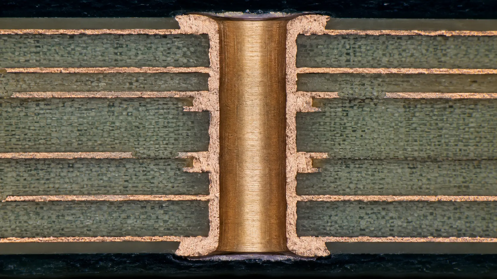
Interpretation rule: Describe what is visible before assigning a cause. A separation at an interface is an observation; deciding whether it resulted from drilling, desmear, plating, lamination, thermal stress, or specimen preparation requires supporting evidence.
4. Plated Holes Need More Than One Number
A single copper-thickness reading is easy to quote and easy to misunderstand. The report should identify the hole or coupon, cut direction, measurement locations, conditioning state, magnification, specification, and result. Local thickness should be interpreted together with continuity, voids, wall quality, inner-layer interfaces, annular geometry, and any applicable thermal conditioning.
The board drawing should distinguish drill size from finished hole size and define whether a feature is plated, non-plated, press-fit, slotted, blind, buried, or a microvia. The PCB hole and slot design guide explains why the manufacturing route changes with the finished function.
Do not copy a generic plating value from another project. IPC-6012F establishes qualification and performance requirements for rigid printed boards, but the applicable class, addendum, deviations, test frequency, conditioning, and customer requirements must be selected in the procurement documentation. Its public table of contents helps locate the relevant subjects; it is not a replacement for the controlled standard.
5. Multilayer and Via Structures Change the Inspection Plan
A conventional through-hole section is not enough to qualify every HDI structure. Blind and buried vias, stacked or staggered microvias, back-drilled holes, copper-filled vias, resin-filled vias, and sequentially laminated constructions may require different coupons, orientations, conditioning, and evidence.
Review the multilayer PCB manufacturing guide for the relationship between stack-up, lamination, drilling and registration. For filled and capped structures, the via-in-pad guide explains why fill, planarization, copper cap, pad surface, and assembly behavior must be considered together.
Common mistake: Requesting “a microsection report” without naming the critical feature. The laboratory may produce a technically clean image of a standard through hole while the actual risk sits in a stacked microvia, back-drill transition, press-fit connector, or local lamination interface.
6. Sampling Determines How Far the Conclusion Can Travel
Microsectioning is local and destructive. One acceptable coupon provides evidence about that coupon and about the processes it was designed to represent; it does not logically prove that every hole or board is identical. Likewise, one failed section does not automatically explain the complete lot until location, repeatability, process history, and comparison samples are investigated.
Traceability should connect the image to the order, part number, revision, lot, panel, coupon, board location, hole or via type, conditioning state, preparation method, inspection date, and evaluator. This is especially important when a report is used for PCB manufacturing quality control or first article approval.
7. A Useful Report Lets Another Engineer Reconstruct the Decision
A report should not consist of one cropped image marked “PASS.” At minimum, it should identify the specimen, revision and lot; purpose of inspection; applicable document and revision; sampling and conditioning; cutting orientation; feature and measurement locations; overview and detailed images; recorded observations and measurements; acceptance result; deviations; and reviewer.
For failure analysis, preserve the original symptom and chain of custody. Record electrical results, photographs, board location, thermal or mechanical history, and nondestructive findings before sectioning. The article on common PCB manufacturing defects provides a broader framework for separating observations, possible causes, verification, containment, and corrective action.
8. What Buyers Should Put in the Purchase Package
Specify the product standard and revision, class and addendum where applicable, board type, special via and hole structures, required coupons, conditioning, sample frequency, characteristics to evaluate, reporting format, retention or delivery of sections, and approval path for deviations. Do not leave these decisions until finished boards are waiting for shipment.
EazyPCB supports PCB fabrication, stack-up and DFM review, prototype and production inspection, and coordination of evidence for special structures. For a project review, contact EazyPCB with the fabrication data, drawing, stack-up, drill table, via definitions, quantity, applicable specification, and required inspection records.
