
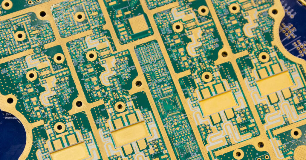
PCB manufacturing is the process of turning circuit board design files into physical printed circuit boards that can be assembled, tested, and used in electronic products. A reliable PCB manufacturing process does more than copy a layout onto material. It checks design data, confirms manufacturability, controls each production step, and verifies quality before shipment.
For engineers, buyers, and project managers, understanding the PCB manufacturing workflow helps reduce delays, avoid redesigns, and communicate requirements more clearly with the supplier. EazyPCB supports PCB fabrication for prototypes and production projects, with engineering review when designs need extra attention.
1. Gerber File Review
The PCB manufacturing process starts with production files. Gerber layers, drill files, board outline, solder mask, silkscreen, paste layers, stack-up notes, impedance requirements, and fabrication drawings should all match the intended design.
A missing drill file or unclear board outline can delay production. Before placing an order, use a Gerber file checklist before PCB manufacturing to confirm that the file package is complete.
2. DFM Review Before Production
DFM, or design for manufacturability, checks whether the board can be built reliably with the selected process. This includes trace width, spacing, hole size, annular ring, solder mask clearance, copper thickness, material, panelization, and special requirements.
A practical PCB DFM checklist helps identify risks before production starts. DFM is especially important for HDI, controlled impedance, heavy copper, rigid-flex, fine-pitch, and high-density PCB manufacturing projects.
3. Material Selection and Stack-Up
PCB material affects electrical performance, thermal behavior, mechanical strength, and long-term reliability. Standard FR-4 is suitable for many designs, while high-TG FR-4, aluminum substrate, Rogers, PTFE, and other materials may be used for special requirements.
The stack-up defines copper layers, dielectric thickness, core and prepreg structure, impedance control, and overall board thickness. For more detail, see our PCB material selection guide.
4. Inner Layer Imaging and Etching
For multilayer boards, inner copper layers are imaged and etched before lamination. The circuit pattern is transferred to copper, unwanted copper is removed, and the remaining traces form the internal connections of the PCB.
This stage requires process control because trace width, spacing, and copper balance can affect electrical performance and manufacturing yield.
5. Lamination
After inner layers are prepared, the PCB stack is laminated under heat and pressure. Core materials, prepreg, and copper foils are bonded into a solid multilayer structure.
For controlled impedance and high-reliability boards, lamination quality and dielectric thickness control are important. Poor stack-up control can affect impedance, board thickness, and mechanical stability.
6. Drilling and Copper Plating
Mechanical drilling or laser drilling creates holes and vias. These holes are then plated with copper so electrical connections can pass between layers. Hole quality, plating thickness, annular ring, and aspect ratio all affect PCB reliability.
If the design uses blind vias, buried vias, microvias, or via-in-pad structures, manufacturing complexity increases. Our PCB via types guide explains how via selection affects PCB manufacturing cost and reliability.
7. Outer Layer Imaging and Etching
After drilling and plating, the outer copper layers are patterned. Copper traces, pads, and other features are defined by imaging and etching.
Copper thickness, trace width, and spacing should match the manufacturer’s capability. If your project includes high-current traces or heavy copper, review the PCB copper thickness guide before releasing the design.
8. Solder Mask and Silkscreen
Solder mask protects copper, improves insulation, and helps prevent solder bridges. Openings are created where pads, test points, and solderable areas must remain exposed. Silkscreen adds reference designators, polarity marks, logos, and assembly information.
Good solder mask registration is important for fine-pitch pads, BGA, and SMT assembly. Poor mask clearance can cover pads or expose too much copper.
9. Surface Finish
Surface finish protects exposed copper and supports solderability. Common PCB surface finishes include HASL, lead-free HASL, ENIG, OSP, immersion silver, and immersion tin.
The right finish depends on cost, shelf life, component pitch, assembly process, and product reliability. Our PCB surface finish guide compares common options used in PCB manufacturing.
10. Electrical Testing and Final Inspection
Finished boards are tested and inspected before shipment. Electrical testing checks for opens and shorts. Visual inspection, dimensional checks, hole inspection, solder mask review, and surface finish inspection help confirm manufacturing quality.
PCB manufacturing quality expectations are often aligned with industry references such as IPC standards, and IPC-A-600 is commonly associated with acceptability of printed boards. For quality management systems, ISO 9001:2015 is also widely recognized.
PCB Manufacturing Tolerances
Every PCB manufacturing process has tolerances. Board thickness, hole size, outline dimensions, copper width, spacing, solder mask registration, and surface finish thickness can vary within acceptable limits.
For projects with tight enclosures, press-fit connectors, card edges, controlled impedance, or high-current requirements, review our PCB manufacturing tolerances guide before production.
From PCB Manufacturing to Assembly
PCB manufacturing and assembly should be planned together when the finished product requires components. Panelization, fiducials, solder mask, surface finish, stencil design, test points, and BOM quality all affect SMT assembly.
If the board will be assembled, it is better to review fabrication and assembly requirements before production starts instead of treating them as separate steps.
Build Reliable PCBs with a Clear Manufacturing Process
A strong PCB manufacturing process connects design review, material selection, production control, inspection, and communication. When these steps are clear, boards are easier to manufacture, assemble, and use reliably in real products.
EazyPCB provides PCB manufacturing support for prototypes, small batches, and production orders with engineering review and quality control. If you need help with manufacturability, stack-up, tolerances, surface finish, or assembly planning, you can contact our team before placing an order.
