Gerber files are the main production data used by PCB manufacturers. They describe copper layers, solder mask, silkscreen, paste layers, drill information, and the board outline. If the Gerber package is incomplete or inconsistent, production may be delayed while the manufacturer asks for clarification.
Before sending your PCB design for fabrication, it is worth spending a few minutes reviewing the file package. A simple checklist can prevent common mistakes, reduce engineering questions, and help your order move into production faster.
1. Confirm the Board Outline
The board outline defines the final shape and size of the PCB. It should be clear, closed, and placed in the correct mechanical layer or outline layer. If your design includes slots, cutouts, rounded corners, or unusual shapes, make sure they are visible and easy to understand.
For complex outlines, it is helpful to include a drawing or note that explains the dimensions and special mechanical requirements.
2. Check Copper Layers
Make sure every required copper layer is included. A 2-layer PCB normally needs top copper and bottom copper. A 4-layer or multilayer PCB needs all internal copper layers exported correctly and named clearly.
Also check that the layer order matches your intended stack-up. Incorrect layer order can cause serious electrical and manufacturing problems, especially for impedance-controlled or power-related designs.
3. Include Drill Files
Drill files define plated through holes, non-plated holes, vias, mounting holes, and other drilled features. Missing or incorrect drill data is one of the most common causes of CAM questions.
Review hole sizes, plated and non-plated hole settings, slot definitions, and drill units. If your design includes castellated holes or special slots, mention them clearly in the order notes.
4. Review Solder Mask and Paste Layers
Solder mask layers determine which copper areas are exposed for soldering. Check that pads are properly opened and that there are no accidental mask openings or missing mask clearances.
Paste layers are important for stencil production and SMT assembly. If you only order bare PCB fabrication, paste layers may not be required, but they are important when you plan PCB assembly.
5. Check Silkscreen Readability
Silkscreen helps identify component positions, polarity, test points, connectors, and revision information. Make sure text is not too small and does not overlap exposed pads. Silkscreen printed over pads may be removed during CAM processing, which can make labels disappear.
For assembly-friendly designs, mark diode polarity, pin 1 orientation, connector direction, and important test points clearly.
6. Verify Manufacturing Specifications
Your Gerber files should match the manufacturing specifications in your order. Confirm board thickness, copper weight, solder mask color, silkscreen color, surface finish, layer count, panelization requirements, and impedance requirements if applicable.
If there is any difference between the Gerber data and the order form, the manufacturer may need to pause the order and ask which information is correct.
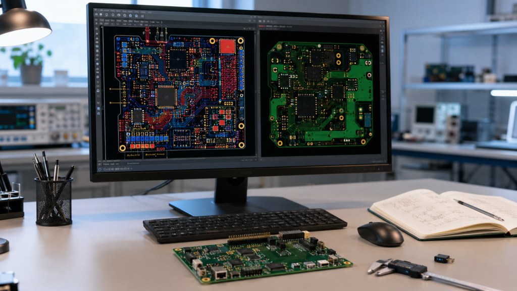
7. Use a Gerber Viewer Before Uploading
Always open the exported files in an independent Gerber viewer before sending them to production. Do not rely only on what you see inside the PCB design software. A viewer helps confirm that the exported files are complete and display as expected.
Check the outline, layers, holes, solder mask, silkscreen, and board size. This final review often catches small export mistakes before they become production delays.
Final Tip: Add Clear Notes for Special Requirements
If your PCB has controlled impedance, heavy copper, special material, blind vias, buried vias, castellated holes, edge plating, or strict tolerance requirements, include clear notes with the order. The more clearly the requirements are communicated, the easier it is for the engineering team to review the job quickly.
EazyPCB supports PCB prototype and production manufacturing with engineering review before fabrication. If you are unsure whether your Gerber files are complete, our team can help check the key production data before your order moves forward.