
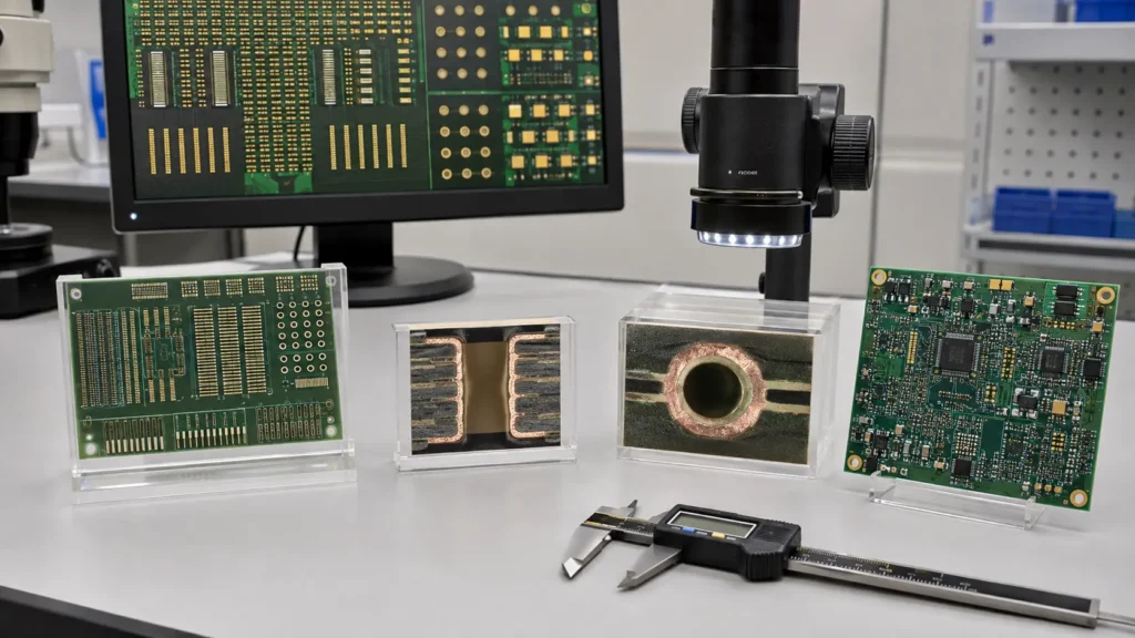
A printed circuit board can look simple from the outside while containing dozens of process-dependent features inside. Imaging, etching, lamination, drilling, copper plating, solder mask, surface finish, profiling, and electrical testing must all remain under control. A weakness in one stage can become an open circuit, short circuit, plating void, delamination, dimensional problem, or field reliability risk.
Understanding common PCB manufacturing defects helps buyers and designers communicate more clearly with suppliers. It also makes defect reports more useful: instead of saying only “the board failed,” the team can identify the affected feature, likely process stage, inspection evidence, and corrective action.
Important distinction: A visible symptom is not always the root cause. An electrical open may come from over-etching, a cracked trace, poor hole plating, contamination, or physical damage. Corrective action should follow evidence, not appearance alone.
1. Separate Bare PCB Defects From Assembly Defects
Bare PCB fabrication creates the unpopulated board. PCBA assembly adds solder paste, components, reflow, through-hole soldering, cleaning, programming, and functional testing. Some symptoms overlap, but the responsible process may be different. For example, a non-functioning circuit may result from an open PCB conductor, an unsoldered component lead, a wrong component, or firmware.
Reviewing the complete PCB manufacturing process helps trace each defect to the stage where it could have been created and the stage where it should have been detected.
| Defect or symptom | Possible cause | Prevention focus | Useful inspection |
|---|---|---|---|
| Open conductor | Over-etch, imaging damage, scratch, weak plated connection | Artwork and etch control, handling, plating control | AOI and electrical test |
| Short circuit | Copper bridge, under-etch, contamination, incorrect data | Spacing review, imaging and etch control, clean processing | AOI and electrical test |
| Annular ring breakout | Registration or drilling offset, insufficient pad allowance | Realistic pad geometry and process capability | Optical and microsection inspection |
| Plating void or thin barrel | Poor hole preparation, chemistry or plating distribution | Desmear, bath control, aspect-ratio review | Electrical test and microsection |
| Delamination or blister | Moisture, contamination, weak bonding, thermal stress | Material storage, surface preparation, qualified lamination | Visual, thermal stress and cross-section review |
| Solder mask misregistration | Artwork alignment or compensation error | Proper mask clearance and registration control | Automated or visual inspection |
| Bow and twist | Asymmetric stack-up, copper imbalance, process stress | Balanced construction and controlled pressing | Flatness measurement |
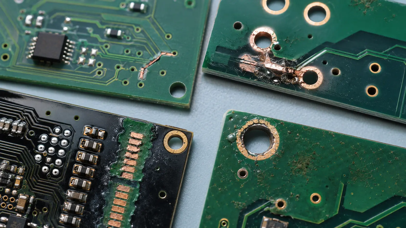
2. Open Circuits, Shorts, and Etching Problems
Inner and outer copper patterns depend on clean imaging and controlled etching. If resist adhesion, exposure, development, copper thickness, chemistry, or conveyor settings drift, conductors may become narrower than intended or unwanted copper may remain between features. Handling scratches can create similar electrical symptoms after imaging.
Good prevention starts with manufacturable line width and spacing, clean production data, controlled equipment, and inner-layer or outer-layer AOI. Electrical testing is the final confirmation that the finished connectivity matches the supplied netlist, but AOI can detect process trends before the panel reaches the end.
3. Annular Ring and Plated Through Hole Defects
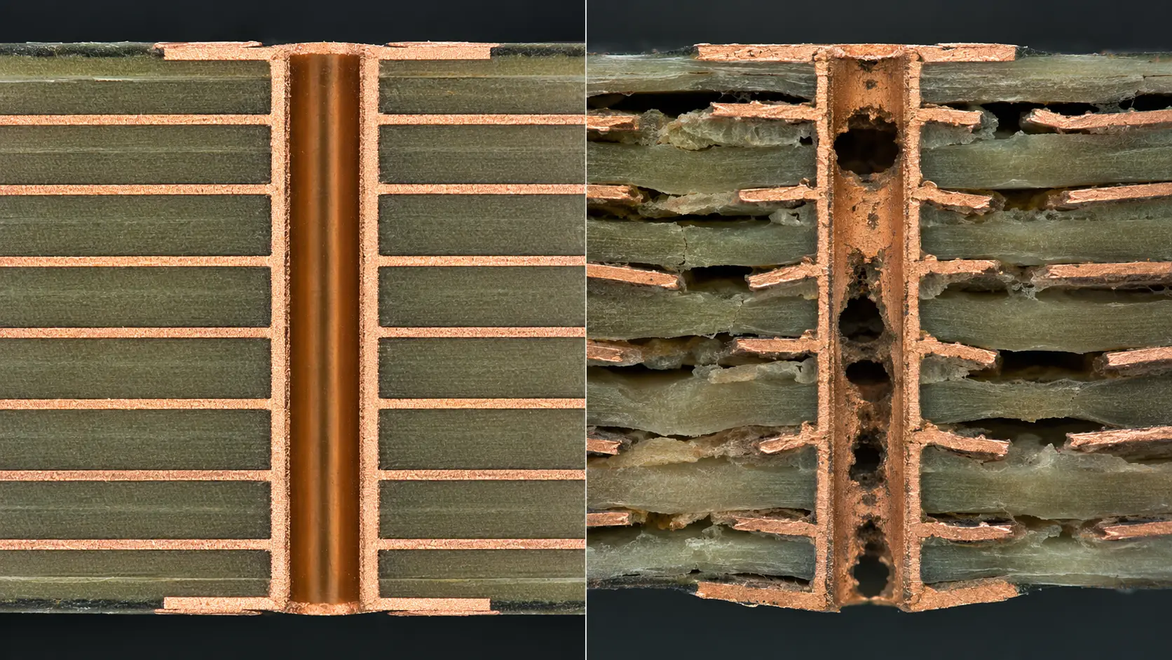
A plated through hole must align with the intended pads and maintain a continuous copper barrel. Drill wander, layer movement, small pad geometry, smear, rough hole walls, plating voids, or insufficient copper can reduce reliability. These risks become more demanding as the board becomes thicker or the hole becomes smaller.
The selected structure also changes the process. Through holes, blind vias, buried vias, and microvias are not interchangeable. Use the PCB via types guide to choose a structure that meets routing needs without adding unnecessary manufacturing risk.
4. Delamination, Blisters, and Lamination Problems
Multilayer bonding depends on compatible materials, clean prepared surfaces, correct prepreg selection, controlled heat and pressure, and proper storage. Moisture or contamination can weaken adhesion. Uneven copper distribution or an unsuitable construction may also influence resin flow, thickness, bow, and twist.
A blister visible on the finished board is only one possible sign. Internal separation may require cross-section, thermal stress, or other agreed verification. Material and process records are important when investigating whether the defect came from incoming laminate, storage, lay-up, pressing, or later thermal exposure.
Investigation rule: Keep failed samples in their original condition whenever possible. Record the board revision, lot number, failure location, test condition, photographs, and electrical symptom before cutting, cleaning, heating, or reworking the sample.
5. Solder Mask and Surface Finish Defects
Solder mask protects conductors and defines exposed pads, but it must be aligned and cured correctly. Common problems include mask on pads, exposed copper beside traces, poor adhesion, pinholes, uneven coverage, and incorrect via tenting. The PCB solder mask guide explains how clearance and fabrication capability affect the result.
Surface finish problems may include uneven coverage, contamination, oxidation, discoloration, or damage that affects solderability or contact performance. Different finishes have different handling and storage needs. Review the PCB surface finish guide before treating HASL, ENIG, OSP, immersion tin, and immersion silver as equivalent choices.
6. Dimensional Errors, Board Outline, and Warpage
A board can pass electrical testing and still fail product assembly because its outline, slots, holes, thickness, edge connector, or flatness does not fit the enclosure. Conflicting drawings and Gerber data, unclear origin points, unrealistic tolerances, routing-tool compensation, and material movement can all contribute.
Critical dimensions should be identified on a controlled drawing rather than left to interpretation. Mechanical requirements should also be reviewed with panelization, breakaway tabs, copper-to-edge clearance, connector fit, and assembly support in mind.
7. Prevent Defects Through DFM and Document Control
Many defects are easier to prevent in the data package than on the factory floor. A PCB DFM review can identify narrow rings, tight spacing, copper near routed edges, conflicting drill data, unsupported via structures, solder mask concerns, and missing fabrication notes before production.
Use revision-controlled Gerber or ODB++ data, drill files, stack-up, fabrication drawing, impedance table, and special requirements. Remove obsolete files from the released package. For unusual materials, copper, thickness, vias, or tolerances, arrange an early review with the PCB fabrication team.
| Control point | Question to answer | Useful evidence |
|---|---|---|
| Incoming material | Is the specified laminate, copper, and thickness being used? | Material identification and receiving records |
| Imaging and etching | Do conductors and spaces match the approved data? | AOI results and process coupons |
| Drilling and plating | Are holes aligned and continuously plated? | Drill records, electrical test, coupon and microsection |
| Final dimensions | Will the board fit its connector and enclosure? | Dimensional report and approved drawing |
| Final acceptance | Which criteria determine accept, repair, or reject? | Inspection plan, test report, agreed standard |
8. Match Inspection to the Defect Risk
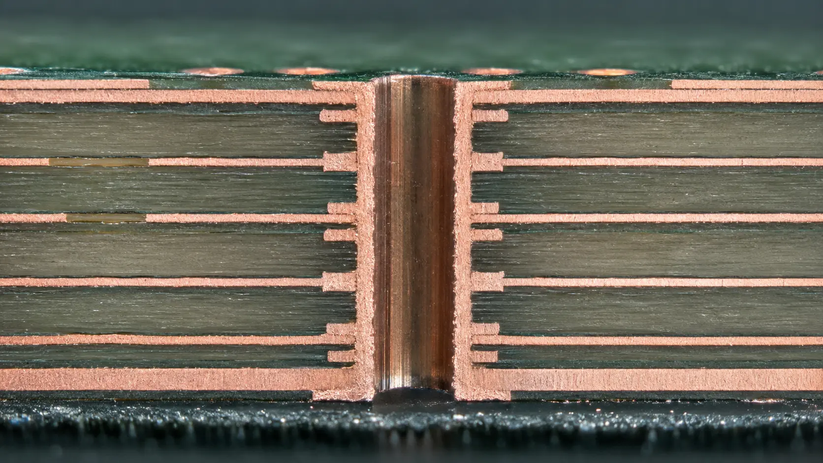
No single inspection method finds every defect. AOI is strong for visible pattern anomalies, electrical testing verifies connectivity and isolation, dimensional tools verify mechanical features, and microsection analysis reveals internal registration and hole plating. Additional testing may be needed when the product has special thermal, voltage, frequency, or reliability requirements.
A documented PCB manufacturing quality control plan should define the test method, sampling or coverage, acceptance criteria, and required records. IPC publishes board design standards and information about printed-board performance and acceptance standards that can support a common buyer-supplier baseline.
Corrective-action checklist: Define the defect, contain the affected lot, preserve evidence, identify the process escape point, verify the root cause, implement corrective action, and confirm effectiveness on later production. Replacing one board without closing the cause is not a complete solution.
Final Thoughts
PCB manufacturing defects are best managed through clear design rules, controlled files, stable processes, suitable inspection, and evidence-based corrective action. The goal is not only to reject bad boards at final inspection, but to prevent the process from creating the defect and to detect drift as early as possible.
EazyPCB supports PCB fabrication, DFM review, prototyping, electrical testing, inspection, and production quality control. To review a defect or prepare a new project, contact EazyPCB with the board revision, manufacturing files, photographs, lot information, and test results.
