HDI PCB stands for high-density interconnect printed circuit board. It is used when a design needs more routing density, smaller board size, finer components, or better electrical performance than a conventional PCB can easily provide.
As electronic products become smaller and more powerful, HDI technology is increasingly used in communication devices, medical electronics, industrial modules, automotive systems, IoT products, and compact consumer electronics.
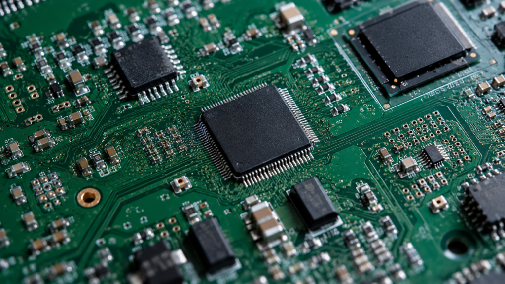
What Makes a PCB an HDI Board?
An HDI PCB typically uses finer traces, smaller spacing, microvias, blind vias, buried vias, and high-density component placement. These features allow more connections to fit into a smaller area.
Compared with standard through-hole via designs, HDI boards provide more routing channels and make it easier to escape signals from fine-pitch BGAs and compact IC packages.
What Are Microvias?
Microvias are very small vias, usually created by laser drilling. They connect adjacent layers or nearby layers in an HDI stack-up. Because they are smaller than mechanical drilled vias, they save space and improve routing flexibility.
Microvias are commonly used for BGA fanout, high-speed routing, compact modules, and designs where standard vias would consume too much space.
Blind Vias and Buried Vias
A blind via connects an outer layer to one or more inner layers but does not pass through the entire board. A buried via connects internal layers and is not visible from the outside. Both are useful when routing density is high and through-hole vias would block too much space.
These via types improve routing freedom, but they also increase manufacturing complexity and cost. They should be used when the design truly needs them.
When Should You Choose HDI PCB?
- The product needs a smaller and lighter PCB.
- The design uses fine-pitch BGA or high-pin-count ICs.
- Routing cannot be completed efficiently with standard through-hole vias.
- The design needs better signal integrity and shorter interconnect paths.
- The board has high component density or strict space constraints.
- The product targets professional, medical, automotive, or high-performance applications.
HDI Stack-Up Planning
HDI design should begin with stack-up planning. The number of layers, microvia structure, dielectric thickness, copper thickness, and lamination sequence all affect manufacturability and cost.
Common HDI structures include 1+N+1, 2+N+2, and more advanced sequential lamination designs. The right choice depends on routing density, BGA pitch, signal requirements, and budget.
Design Considerations for HDI Boards
- Confirm minimum trace width and spacing with your PCB manufacturer.
- Check minimum microvia diameter and laser drilling capability.
- Plan BGA fanout strategy before placing components.
- Avoid unnecessary via stacking unless the design requires it.
- Keep high-speed signals close to stable reference planes.
- Discuss impedance control and material selection early.
Cost and Manufacturing Trade-Offs
HDI PCBs can reduce board size and improve routing, but they are more complex to manufacture than standard PCBs. Laser drilling, sequential lamination, tighter tolerances, and advanced inspection can increase cost and lead time.
For this reason, HDI should be chosen when it solves a real design problem: size, density, signal quality, BGA escape routing, or product performance.
Work with an Experienced HDI PCB Manufacturer
Successful HDI manufacturing requires coordination between design and fabrication. Early review of stack-up, microvia rules, materials, impedance targets, and tolerance requirements can prevent costly redesigns.
EazyPCB supports prototype and production PCB manufacturing, including advanced multilayer and high-density designs. If your product requires microvias, fine-pitch routing, BGA fanout, or compact board architecture, our team can help review the key manufacturing requirements before production.