
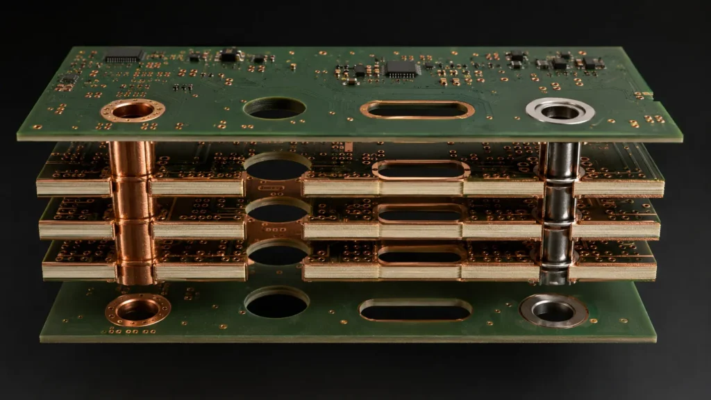
A connector pin can be correct, the board outline can be correct, and the assembly can still stop because one hole was described ambiguously. A note such as “1.0 mm hole” does not tell the fabricator whether 1.0 mm is the drill tool or the finished diameter, whether the wall must be plated, or whether the hole belongs to a press-fit interface with its own acceptance requirements.
Good PCB manufacturing data treats holes and slots as functional features rather than a list of coordinates. The fabrication drawing, drill files, pad geometry, component specification, and assembly plan should all describe the same intent. A focused PCB DFM review can then identify conflicts before tooling begins.
Start with function: Decide what each hole does before choosing its manufacturing description. A soldered lead, mounting screw, locating pin, via, plated slot, and press-fit contact do not have interchangeable requirements.
1. Classify Every Hole by Function and Plating Status
A plated through hole (PTH) has a conductive barrel and may connect copper layers, accept a component lead, or perform both jobs. A non-plated through hole (NPTH) is normally a mechanical feature without a conductive barrel. Slots can also be plated or non-plated, so shape alone does not define their purpose.
The distinction affects process sequence, copper clearance, inspection, and the final opening. It should be visible in the CAD data and fabrication documentation, not left for the CAM operator to infer from nearby pads.
| Feature | Typical purpose | What the data must clarify |
|---|---|---|
| PTH component hole | Soldered lead plus electrical connection | Finished size, tolerance, pad, connected layers, lead fit |
| NPTH mounting hole | Fastener, alignment, or mechanical clearance | Finished size, position, copper keep-out, mechanical tolerance |
| Via | Electrical layer transition | Via type, finished requirement, pad and anti-pad geometry |
| Plated slot | Flat lead, tab, shield, or special connector | Finished width and length, plating, endpoint geometry, tolerance |
| Press-fit hole | Compliant-pin mechanical and electrical interface | Connector specification, finished hole range, plating system, board construction |

2. Specify Finished Hole Size, Not an Assumed Drill Tool
For a plated hole, copper deposition changes the opening after drilling. The fabricator normally selects a drill tool and process compensation that will achieve the required finished size. If the drawing gives only a nominal drill value while the component drawing gives a finished-hole range, the two documents may conflict even though each looks reasonable by itself.
State the finished diameter and tolerance for fit-critical features. Let the manufacturer select the production drill unless the tool size itself is contractually important and has been agreed. For ordinary vias, use the supplier’s supported design rules; for component and mechanical interfaces, work backward from the lead, pin, screw, or locating feature.
Common documentation trap: Do not mix finished hole size, nominal CAD drill, and manufacturing tool diameter in one unlabeled column. Name the value explicitly and define whether the tolerance applies before or after plating.
3. Treat Annular Ring, Registration, and Copper Clearance as One Geometry
A finished hole cannot be reviewed in isolation. The pad must retain suitable copper around the drilled opening after normal registration and process variation. On inner planes, the anti-pad also needs enough clearance to prevent an unintended connection. Reducing only the drill without checking the pad, anti-pad, aspect ratio, and assembly need can move risk rather than remove it.
This relationship is especially important for dense multilayer boards. The broader PCB via guide explains how through, blind, buried, and microvia structures change the manufacturing sequence. IPC lists IPC-2221 as the generic printed-board design standard and IPC-2222 as the sectional design standard for rigid organic boards in its design standards overview.
4. Define Slots and Cutouts With Manufacturable Geometry
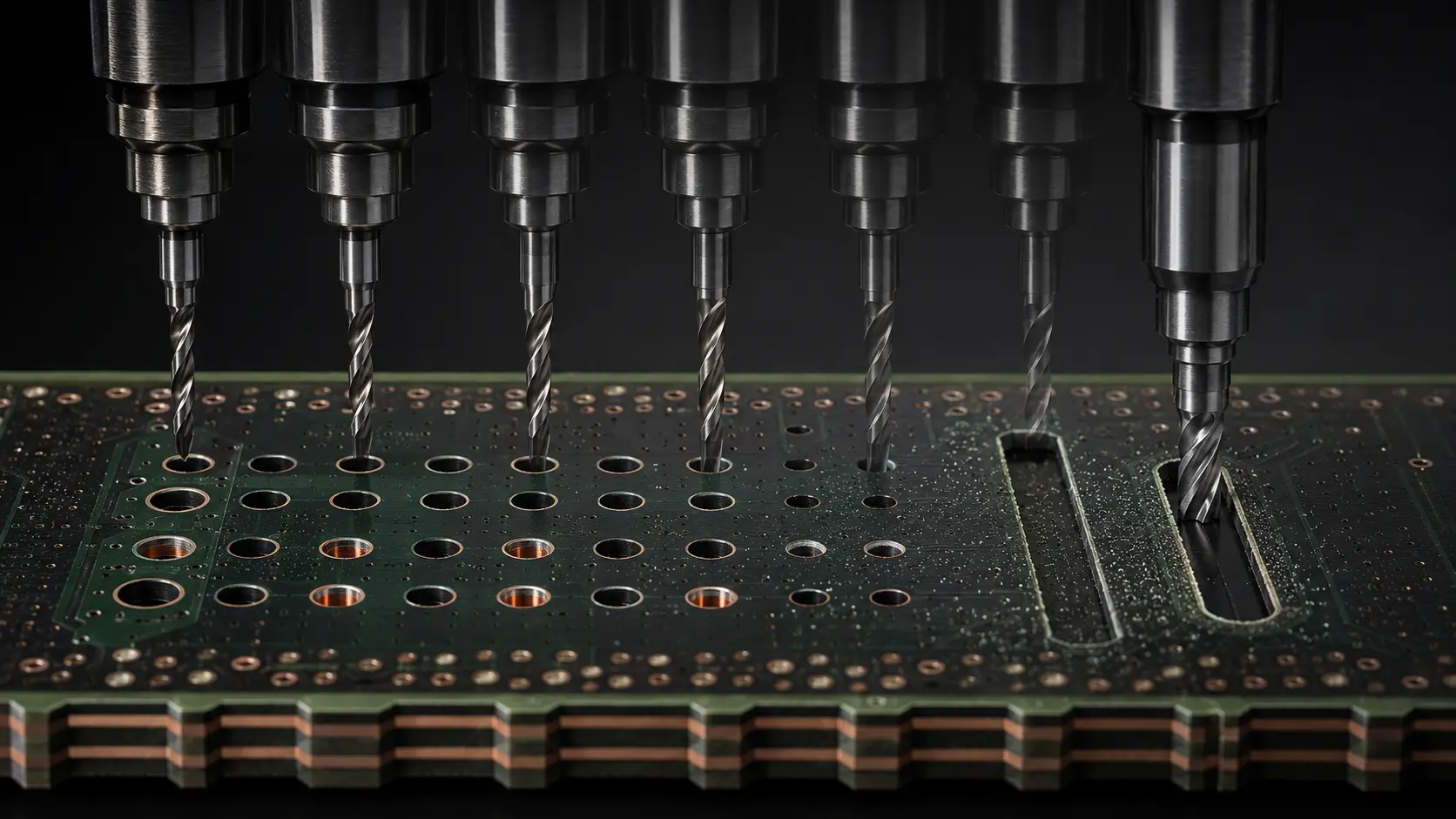
An elongated opening may be generated by routing, repeated drilling, or another agreed method. The chosen process affects the minimum practical width, endpoint shape, edge quality, and tolerance. A dimensioned mechanical drawing should state finished width and length, location, whether the slot is plated, and any endpoint or corner requirement that affects component fit.
Do not rely on a line drawn on a Gerber layer without identifying its meaning. The same line might be interpreted as a board outline, centerline, keep-out, or route path. If a slot accepts a flat terminal, compare the complete terminal tolerance with the finished slot range and the soldering process.
5. Press-Fit Holes Need the Connector Specification
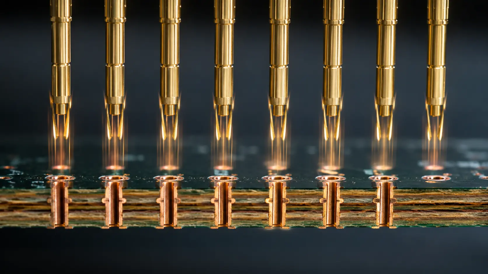
A press-fit interface is not a generic PTH with a tight diameter. Contact geometry, finished hole range, copper and surface finish, board thickness, insertion tooling, and acceptance method belong to one system. The correct values come from the exact connector manufacturer’s drawing and application specification.
TE Connectivity’s press-fit connection catalog, for example, associates specific contact designs with product specifications and nominal PCB hole diameters. That is a useful reminder not to copy a hole value from a different pin family. Share the manufacturer, complete part number, revision, and applicable specification with the PCB fabrication supplier.
Do not approve by diameter alone: A measured hole can be within range while barrel condition, plating system, insertion setup, or board support is wrong. Define the evidence needed for both the bare board and the assembled connector.
6. Make the Drill Package Self-Consistent
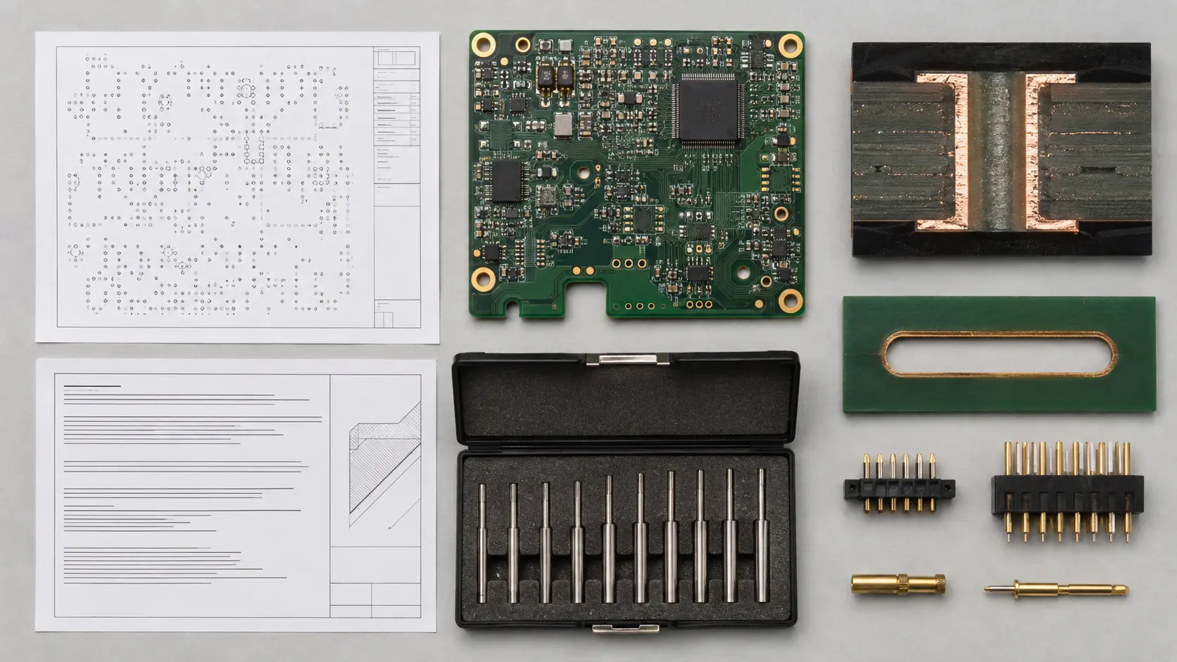
The released package should contain the correct drill data, fabrication drawing, board outline or route data, stack-up, and revision identification. The drill map is useful for human review, but the machine-readable files and drawing notes must agree with it.
KiCad’s official drill-file documentation notes that PTH and NPTH holes are generated in separate files by default and that oval holes are normally represented with route commands. Whatever CAD system is used, review the exported deliverables rather than assuming the database settings survived export correctly.
| Possible conflict | Manufacturing risk | Release check |
|---|---|---|
| Drawing says NPTH; pad stack is plated | Wrong process interpretation or copper remaining near the hole | Match plating status across CAD, drill files, and drawing |
| Hole table and component drawing use different sizes | Loose fit, interference, or assembly stoppage | Identify the governing finished-hole requirement |
| Slot shown only as an unlabeled line | Missing, incorrectly sized, or incorrectly plated slot | Add dimensions, route data, plating status, and location |
| Press-fit note lacks connector revision | Use of requirements from the wrong contact family | Attach the exact vendor specification and part number |
| Mixed coordinate origins or revisions | Shifted features or a hybrid of two design releases | Plot all files together and verify archive identity |
7. Inspect According to the Risk of the Interface
Visual review can confirm whether holes and slots exist and whether obvious damage is present. Dimensional measurement can verify selected finished openings and locations. Microsection evidence may be specified when plated-hole structure must be evaluated. Assembly trials can verify pin, lead, fastener, or enclosure fit, but they do not replace every bare-board acceptance check.
IPC-6012F defines qualification and performance requirements for rigid printed boards, including constructions with plated through holes, as shown in its official scope and contents. Confirm the applicable document revision through the IPC revision table, then state the product class, customer exceptions, inspection frequency, and order-specific requirements in the procurement package.
Buyer release checklist:
- Each special hole and slot has a stated function and plating status.
- Fit-critical dimensions are identified as finished sizes with tolerances.
- Pad, anti-pad, copper clearance, and board stack-up support the feature.
- Press-fit requirements cite the exact connector and vendor document revision.
- Drill files, route data, drawing, map, and archive revision agree.
- The inspection and assembly-fit evidence is defined before production.
Final Thoughts
Reliable hole design is less about choosing one “safe” diameter and more about keeping mechanical fit, copper geometry, plating, tooling, data output, and inspection aligned. When those elements disagree, the final board may be electrically sound yet impossible to assemble.
EazyPCB supports PCB fabrication, DFM review, prototypes, hole and slot review, inspection coordination, and PCB assembly services. For a design with press-fit contacts, plated slots, controlled finished holes, or unusual mechanical interfaces, contact EazyPCB with the released fabrication package, component drawings, connector specifications, critical dimensions, quantity, and required evidence.
“`
