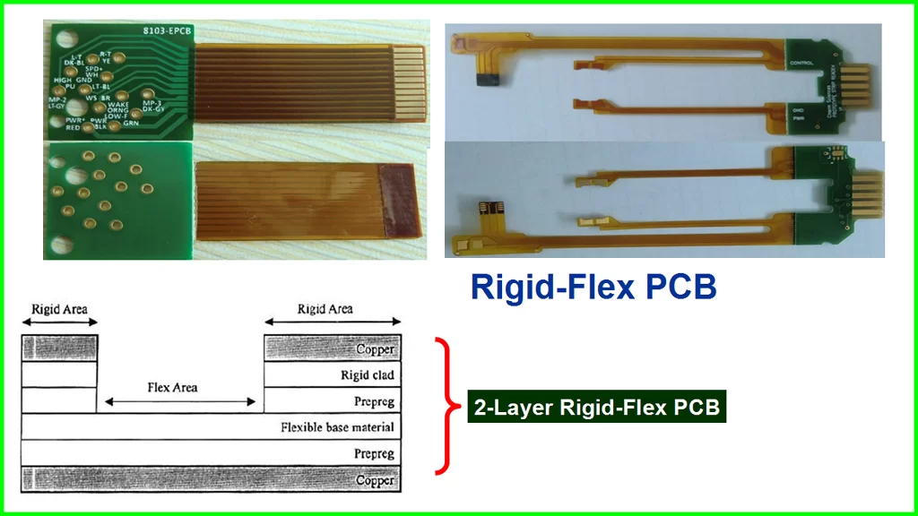
Rigid Flex PCB
Manufacturing multilayer PCB up to 56 layer, IPC III Standard, Multilayer Rigid PCB, Multilayer Flex PCB, Rigid-flex Board, hybrid PCB…
Personal Information

Introduction
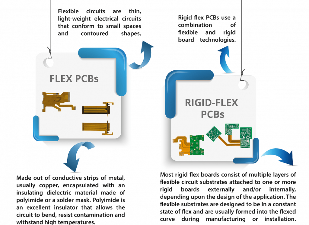
Rigid Flex PCBs, a hybrid of rigid and flexible circuit boards, are a transformative solution in modern electronics. These PCBs integrate the stability and robustness of rigid boards with the adaptability and weight reduction of flexible circuits. This unique combination allows them to address the growing demands for compact, lightweight, and high-performance electronic systems.
Applications of Rigid Flex PCBs span various industries, including aerospace, automotive, medical, military, and consumer electronics. Their ability to withstand extreme conditions, reduce assembly complexity, and enhance system reliability makes them indispensable in designing advanced electronic devices.
Unlike separate rigid and flexible circuits connected through connectors or cables, Rigid Flex PCBs eliminate interconnects, simplifying designs, enhancing signal integrity, and reducing failure points. As technology evolves, Rigid Flex PCBs are set to play a pivotal role in next-generation devices.
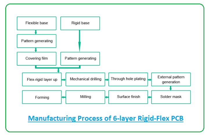
1. Rigid Flex PCB's Manufacturing Process Introduction
Manufacturing Rigid Flex PCBs involves precise engineering and a series of sophisticated steps to ensure performance and reliability:
Substrate Preparation:
Flexible PCBs use thin layers of polyimide (PI) or polyester (PET) films as substrates due to their flexibility and thermal stability. These films are cleaned and treated to ensure good adhesion.Copper Cladding:
A copper layer is laminated onto the substrate using either adhesive bonding or a direct deposition process. Adhesive-free laminates are preferred for high-performance applications as they offer better thermal and electrical properties.Circuit Patterning:
Photolithography or laser etching is used to define circuit patterns. A photoresist is applied, exposed to UV light through a mask, and developed to leave behind the desired copper paths.Etching and Stripping:
Unnecessary copper is etched away using chemical solutions, leaving only the circuit traces.Drilling and Plating:
Precision drilling methods such as laser drilling create microvias for interconnections. The vias are then plated with copper for conductivity.Coverlay and Finishing:
Protective layers, such as polyimide coverlays or solder masks, are applied to shield the circuit from environmental factors like moisture, dust, and chemicals.Inspection and Testing:
Comprehensive electrical and visual inspections are conducted to ensure quality and reliability.
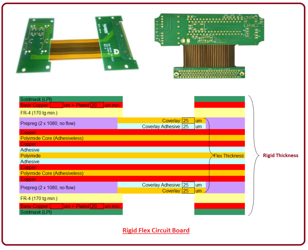
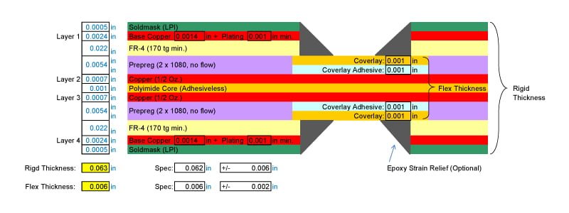
2. Rigid Flex PCB's Materials and Structure Introduction
The unique structure of Rigid Flex PCBs is the key to their versatility and functionality.
Materials Used:
Flexible Sections:
- Substrates: Polyimide (PI) or polyester (PET) films, chosen for their flexibility, thermal stability, and durability.
- Coverlays: Polyimide-based layers protect circuits from mechanical stress and environmental damage.
Rigid Sections:
- Core Material: FR4 or high Tg materials provide strength and stability for mounting components.
- Prepreg Layers: Resin-impregnated fiberglass sheets are used for lamination.
Conductive Layers:
- Copper foils with varying thicknesses (1oz, 2oz, etc.) are used depending on current-carrying requirements.
Adhesives:
- Epoxy or acrylic adhesives bond rigid and flexible layers. Adhesive-free laminates are ideal for high-reliability applications.
Structure:
Rigid Flex PCBs consist of alternating rigid and flexible sections, with smooth transitions designed to minimize mechanical strain. Flexible areas act as connectors, eliminating the need for cables or connectors.
3. Rigid Flex PCB's Design Considerations Introduction
Designing Rigid Flex PCBs requires addressing both mechanical and electrical challenges:
Key Considerations:
Bend Radius:
- Flexible sections must maintain a minimum bend radius (usually 10–15 times the flex thickness) to prevent cracking and delamination.
Trace Layout:
- Avoid sharp angles; use curved or staggered traces to reduce mechanical stress.
Layer Balancing:
- Symmetrical stackups prevent warping during thermal cycles.
Transition Zones:
- Ensure gradual transitions between rigid and flexible sections to avoid stress concentrations.
Via Placement:
- Keep vias away from bend zones and reduce the number of vias in flexible areas.
Component Placement:
- Limit heavy components to rigid sections, and use stiffeners if necessary.
Thermal Management:
- Include provisions for heat dissipation, especially in high-power designs.
4. Modeling and Analysis
Simulation and modeling tools are essential for ensuring the performance and reliability of Rigid Flex PCBs:
3D CAD Models:
- Enable visualization of the board in its operational configuration, ensuring accurate fit and alignment.
Mechanical Stress Analysis:
- Finite Element Analysis (FEA) simulates stress distribution in bending zones, ensuring durability over repeated flexing cycles.
Thermal Analysis:
- Predicts temperature profiles and helps optimize heat dissipation.
Dynamic Simulations:
- Evaluate performance under motion, ensuring the design meets operational requirements in dynamic applications.
5. Signal Integrity Considerations
Rigid Flex PCBs are often used in high-speed and high-frequency applications, where signal integrity is paramount:
Controlled Impedance:
- Maintain uniform trace widths and consistent dielectric thickness across rigid and flexible sections.
Ground Planes:
- Use ground planes to reduce noise and improve signal stability.
Crosstalk Reduction:
- Optimize trace spacing and consider shielding for sensitive signals.
Via Optimization:
- Minimize vias and use optimized via structures to reduce signal reflections and loss.
EMI/EMC Control:
- Add shielding layers or materials to minimize electromagnetic interference.
6. Cost Considerations
While Rigid Flex PCBs offer significant advantages, their complex manufacturing process and material requirements result in higher costs.
Strategies to Control Costs:
Simplify Design:
- Avoid unnecessary layers and minimize the use of flexible sections.
Material Selection:
- Use cost-effective materials while ensuring they meet application requirements.
Panel Optimization:
- Design panel layouts to maximize material usage and reduce waste.
Batch Production:
- Larger production volumes reduce per-unit costs.
Collaborate with Manufacturers:
- Engage with experienced PCB manufacturers early in the design phase to optimize for cost and performance.
7. Conclusion
Rigid Flex PCBs represent the pinnacle of modern PCB technology, combining the strengths of rigid boards and flexible circuits into a unified solution. Their unique advantages—reduced assembly complexity, enhanced signal integrity, and greater reliability—make them indispensable in high-performance, space-constrained applications.
Understanding the materials, manufacturing processes, and design considerations enables engineers to unlock the full potential of Rigid Flex PCBs while balancing performance and cost. As industries continue to push the boundaries of technology, Rigid Flex PCBs will remain a cornerstone of innovation.
Contact
805, Block A, Guangming Centre, No. 2, Chuangming Road, Yongning Street, Zengcheng District, Guangzhou, China
- op@eazypcb.com
- Eazypcb
- +86 13342868540