PCB Manufacturing &
Assembly Capabilities

ABOUT US
20 Years PCB Manufacturer
EAZYPCB specializes in the latest advancements in printed circuit board (PCB) manufacturing technologies, delivering top-tier quality standards to meet the evolving demands of the electronics industry. With successful collaborations spanning over 6000 high-tech R&D, manufacturing, and service companies across sectors such as telecommunications, industrial automation, medical electronics, automotive, semiconductor, rail transportation, and more, eazypcb has built a reputation for excellence.
At the core of eazypcb’s philosophy is the pursuit of technological innovation. Our dedicated innovation labs and engineering teams continuously tackle emerging challenges in PCB design, focusing on areas like High-Speed and High-Capacity Circuits, RF and Microwave Technologies, Thermal Management, Miniaturization, and Chip Packaging Substrates. We are committed to overcoming these design obstacles to deliver solutions that set the standard in the industry.
PCB Manufacturing Type

Metal PCB

HDI PCB

ROGERS PCB

CERAMIC PCB

FLEXIBLE PCB

RIGID FLEX PCB
PCB OUR SERVED

- White PCB
- Black PCB
- Matte PCB
- Yellow PCB
- Blue PCB
- Purple PCB
- Orange PCB
- HDI PCB
- Rigid-Flex PCB
- High Frequency PCB
- Hybrid PCB
- Flexible PCB
- Impedance Control PCB
- Heavy Copper PCB
- Blind via PCB
- Press Fit Hole PCB
- Cavity PCB
- Via in Pad PCB
- Castellated holes PCB
- Carbon Ink PCB
- Countersink Holes
- Back drill PCB
- High TG PCB
- Ultra thin PCB
- Embedded copper PCB
- Antenna PCB
- Edge plating PCB
- Medical PCB
- Industrial PCB
- Military PCB
- NFC PCB
- Led PCB
- BMS PCB
- Robotics PCB
- IOT Device PCB
- Aerospace PCB
- Automotive PCB
- POWER PCB
- Measuring Equipment
- Telecommunications PCB
- Smart Home PCB
- Audio PCB
- Wearable pcb
- High Speed and High Capacity
- RF and Microwave
- 12 Layer PCB
- 10 Layer PCB
- 8 Layer PCB
- 6 Layer PCB
- 4 Layer PCB
- 24 Layer PCB
- 32 Layer PCB
- 2 Layer PCB
- 1 Layer PCB
- 14 Layer PCB
- 28 Layer PCB
- 52 Layer PCB
- 100 Layer PCB
- HASL-LF PCB
- Immersion Gold PCB
- Immersion Tin PCB
- Immersion Silver PCB
- ENEPIG PCB
- OSP PCB
- Nickel PCB
- Soft Gold PCB
- Electrolytic Hard Gold PCB
- 0.1mm PCB
- 0.2mm PCB
- 0.4mm PCB
- 0.6mm PCB
- 0.8mm PCB
- 1.0 mm PCB
- 1.2mm PCB
- 1.6mm PCB
- 1.8mm PCB
- 2.0mm PCB
- 2.4mm PCB
- 2.8mm PCB
- 3.2mm PCB
- 4.8mm PCB
- 5.6mm PCB
- 10.0mm PCB
- White PCB
- Black PCB
- Matte PCB
- Yellow PCB
- Blue PCB
- Purple PCB
- Orange PCB
- 1/2 Half Oz PCB
- 1 Oz PCB
- 2 Oz PCB
- 3 Oz PCB
- 4 Oz PCB
- 6 Oz PCB
- 8 Oz PCB
- 10 Oz PCB
- 20 Oz PCB
- 30 Oz PCB
Why Choose Us
Our Process Capabilities
Item | Manufacturing Capability | Technical Details | Graphical Explanation |
---|---|---|---|
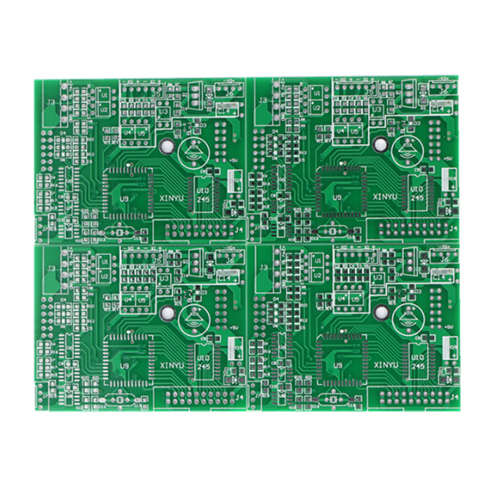
Layer Count | 2 layers | Layer count refers to the number of electrical layers (copper layers) in the PCB | Currently, we only accept 2-layer through-hole boards (no buried or blind vias) |
Board Material | FR-4 material | All fiberglass (FR-4) six/four-layer glass fabric | ![]() |
Overall Process | Maximum Size | 122cm*55cm | Both sides cannot exceed 55cm simultaneously (one side can be 122.9cm, the other must be <55cm) |
Solder Mask Type |
Photoimageable ink
Green
Blue
Red
Yellow
White
Black
|
Photoimageable ink is the most commonly used type; heat-resistant ink is generally used for low-grade single-sided paper boards | |
Finished Outer Layer Copper Thickness | 1oz, default standard PCB outer layer copper foil circuit thickness is 1oz | ||
Board Thickness Range | 0.8~1.6mm | Current production board thicknesses: 0.8/1.0/1.2/1.6mm | |
Finished Product | Board Thickness Tolerance |
Board thickness ≥1.0mm, tolerance +/-10% Board thickness <1.0mm, tolerance +/-0.1mm |
For example, if board thickness T=1.6mm, actual thickness range: 1.44mm (T-1.6×10%) ~ 1.76mm (T+1.6×10%); If board thickness T=0.8mm, actual thickness range: 0.7mm (T-0.1) ~ 0.9mm (T+0.1) |
V-cut Panel Delivery | Distance between traces/pads and board edge: ≥0.4mm | Traces must be 0.4mm away from the edge, otherwise V-cut may damage circuits and pads | |
Single Board Delivery | Distance between traces/pads and board edge: ≥0.2mm | Single board delivery requires ≥0.2mm clearance, otherwise it may affect internal circuits and pads | |
Drilling | Drill Hole Diameter (Mechanical Drilling) | 0.2~6.3mm | Minimum hole diameter 0.2mm, maximum 6.3mm. Holes larger than 6.3mm require special processing. Mechanical drill bit specifications increase in 0.05mm increments, e.g., 0.25, 0.3mm |
Hole Diameter Tolerance (Mechanical Drilling) | +/-0.075mm | Drilling tolerance is +/-0.075mm. For example, a 0.6mm designed hole will have an actual finished hole diameter between 0.525~0.675mm | |
Minimum Via Inner and Outer Diameter |
Minimum inner diameter: 0.2mm Minimum outer diameter: 0.45mm |
Multilayer board minimum inner diameter: 0.2mm, minimum outer diameter: 0.45mm Double-sided board minimum inner diameter: 0.2mm, minimum outer diameter: 0.45mm |
|
Via Single-side Annular Ring | 5mil | ||
Traces | Trace Width | 3.5mil for single-sided, double-sided, and multilayer boards | ![]() |
Trace Spacing | 4mil for single-sided, double-sided, and multilayer boards | ![]() |
|
Pad Edge to Trace Edge Spacing | 8mil | ![]() |
|
Characters | Minimum Character Width |
Line width: 4mil Character height: 27.5mil |
![]() |
V-CUT | Minimum V-CUT to Trace Distance | ≥0.5mm | |
V-CUT Offset | ±0.15mm | ||
V-CUT Remaining Thickness | As per customer requirements, if not specified, 1/3 of board thickness | ±10% | |
V-CUT Angle | As per customer requirements, if not specified, 30° blade is used | 25-30° | |
V-CUT Upper and Lower Blade Alignment | ±0.05mm | ||
V-CUT Upper and Lower Depth Difference | ±0.1mm | ||
External Dimensional Accuracy | ±0.15mm | Board outline tolerance +/-0.15mm | |
Minimum Fabrication Border | 3mm | ||
Notes | Pads Manufacturer Copper Pour Method | Hatch method for copper pour | |
Drawing Slots in Pads Software | If there are many non-metallized slots on the board, please use outline to draw |
PCB Manufacturing Knowledge
- 10 Essential PCB Manufacturing Processes You Need to Know
- How Material Selection Impacts PCB Performance and Cost
- Step-by-Step Guide to Multilayer PCB Manufacturing
- The Role of DFM (Design for Manufacturing) in PCB Production
- Understanding PCB Copper Thickness: Standards and Applications
- HDI PCB Manufacturing: Techniques and Benefits Explained
- Key Differences Between Rigid, Flex, and Rigid-Flex PCBs
- Top Challenges in PCB Manufacturing and How to Overcome Them
- Why Via Design is Critical in PCB Manufacturing
- An Overview of PCB Surface Finishes: ENIG vs. HASL and More
- PCB Prototyping vs. Mass Production: Key Considerations
- Green Manufacturing in PCB Production: Eco-Friendly Practices
- The Importance of PCB Testing and Quality Assurance
- How Automation is Revolutionizing PCB Assembly
- Thermal Management Techniques in High-Power PCBs
- The Future of PCB Manufacturing: AI and IoT Integration
- How to Optimize PCB Design for High-Speed Applications
- Understanding the Role of Solder Mask in PCB Manufacturing
- Common Defects in PCB Manufacturing and How to Avoid Them
- Choosing the Right PCB Manufacturer: A Comprehensive Guide