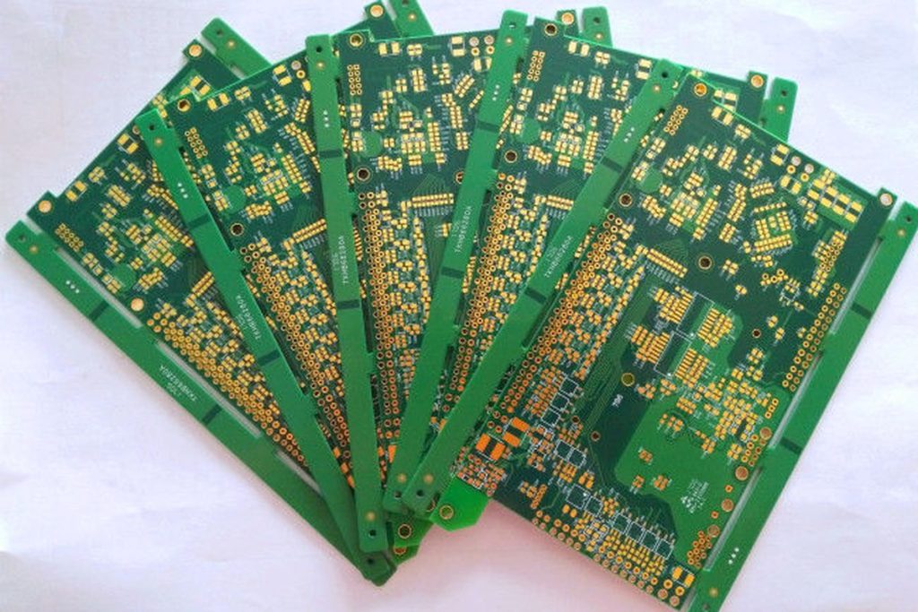
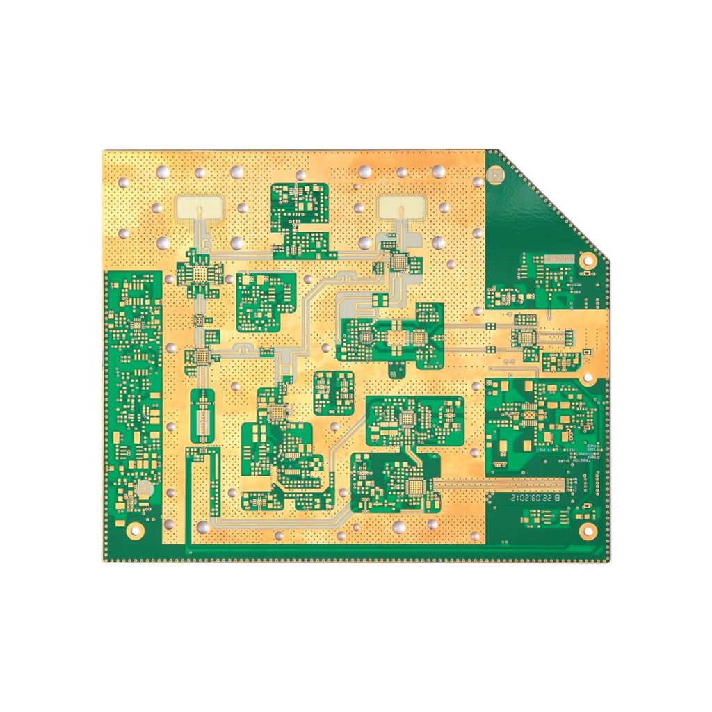
Multilayer PCB
Manufacturing multilayer PCB up to 56 layer, IPC III Standard, Multilayer Rigid PCB, Multilayer Flex PCB, Rigid-flex Board, hybrid PCB…
Personal Information

Introduction
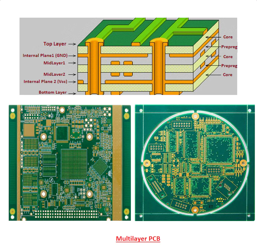
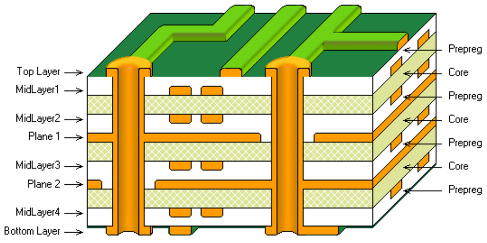
A multilayer printed circuit board (PCB) consists of two or more conductive copper layers separated by insulating dielectric materials like FR-4. These PCBs allow for greater component density by enabling component placement on both external surfaces and within internal buried layers. They are widely utilized in advanced digital systems, RF/microwave applications, high-speed computing, and other scenarios demanding high levels of interconnectivity.
This article offers a comprehensive guide to multilayer PCB technology, discussing topics such as:
- Manufacturing processes for multilayer PCBs
- Materials and structural design
- Critical design considerations
- Modeling and simulation
- Thermal performance optimization
- Signal integrity challenges
- Cost-benefit analysis
- Reliability considerations
Gaining a solid understanding of multilayer PCB capabilities and design principles is crucial for maximizing their advantages in electronic product innovation.
Multilayer PCB Manufacturing Process
Producing a multilayer PCB involves advanced sequential lamination techniques to fuse multiple double-sided circuit layers into a single cohesive board. The typical manufacturing process includes the following steps:
Inner Layer Preparation
- Use photolithography to define circuit patterns on copper-clad laminates.
- Etch away excess copper, leaving only the required traces.
- Add registration marks and tooling holes for alignment.
- Perform electrical testing of the traces.
- Prepare the surfaces for lamination through cleaning or treatment.
Layer Lamination
- Utilize lamination presses to bond the layers into a stack.
- Arrange the stackup with cores, prepregs, copper, and dielectric materials.
- Cure the assembly under controlled temperature and pressure to form a solid laminate.
Drilling
- Precisely drill tooling and via holes using high-accuracy equipment.
- Ensure accurate alignment for proper hole placement through all layers.
Hole Plating
- Deposit a thin conductive layer using electroless copper plating.
- Build up the copper thickness through electrolytic plating, connecting inner layers and drilled vias.
Outer Layer Processing
- Apply a liquid photoimageable (LPI) solder mask to protect the board.
- Print legends for identification and labeling.
- Pattern and etch outer layers to create external circuits.
- Route the panel to separate it into individual PCBs.
Testing and Quality Assurance (QA)
- Conduct automated optical inspection (AOI) for defect detection.
- Verify net connectivity and impedance through electrical testing.
- Perform high-voltage and functional tests as needed.
- Check dimensions and tolerances for quality compliance.
Multilayer PCB Materials and Construction
Multilayer PCBs are composed of conductive copper layers separated by dielectric materials, including prepregs and core layers. Below are common material choices:
Conductive Layers
- Rolled annealed copper foil with thicknesses ranging from ½ oz to 3 oz.
- Electrodeposited copper foil for enhanced performance.
- Finishes such as silver, gold, or nickel plating for improved durability and conductivity.
Dielectric Layers
- FR-4: A glass-reinforced epoxy commonly used for its reliability and cost-effectiveness.
- High Tg Epoxy: Designed for stability under high-temperature conditions.
- PTFE (Teflon): Ideal for RF and wireless applications due to low dielectric loss.
- Polyimide: Suitable for flexible PCB designs.
- Cyanate Ester: Preferred for radar and defense systems requiring high performance.
Bonding Layers
- FR-4 Prepregs: Partially cured resin sheets for bonding.
- Rogers Prepregs: Known for superior electrical properties.
- Fluoropolymer Adhesive Films: Used for advanced dielectric properties.
- Both reinforced and non-reinforced options are available to meet specific design requirements.
Common Multilayer Constructions
- 4-6 Layers: For low to moderately complex designs.
- 8-10 Layers: Suitable for higher complexity in digital circuits.
- 12-16 Layers: Used in advanced RF and data processing applications.
- 20+ Layers: Designed for dense interconnects in high-performance systems.
- 60+ Layers: Represents cutting-edge HDI (High-Density Interconnect) technology for state-of-the-art applications.
Multilayer PCB Design Considerations
Designing multilayer PCBs requires careful consideration of factors such as interconnect density, thermal management, manufacturing limitations, and signal integrity. Below are essential guidelines for effective multilayer PCB design:
Board Stackup
- Select dielectric materials based on their electrical properties, thermal performance, and coefficient of thermal expansion (CTE).
- Simulate the stackup performance using various laminate combinations.
- Maintain symmetric layer construction whenever feasible to prevent warping.
- Include reference planes for each signal layer to enhance stability.
- Assign layers strategically for power, ground, and signal to optimize functionality.
High-Speed Routing
- Implement impedance-controlled traces for high-speed signals.
- Route sensitive traces between ground or power planes to reduce interference.
- Match trace widths and spacing for differential pairs.
- Avoid sharp bends, stubs, and mismatched trace lengths.
- Simulate high-speed performance in the intended operating environment.
Thermal Design
- Identify and manage hot spots using heat spreading layers.
- Include thermal vias to facilitate heat dissipation.
- Employ thicker copper layers for better heat spreading.
- Choose dielectrics with high thermal conductivity.
- Ensure adequate spacing for components and proper airflow to aid cooling.
Signal Integrity
- Optimize the stackup to minimize noise and coupling.
- Assign return paths for all high-speed traces to maintain signal quality.
- Use plated-through holes to ensure consistent signal returns.
- Add passive components like capacitors and resistors to improve signal stability.
- Include decoupling and termination provisions to manage transients.
Power Distribution
- Provide sufficient pins to accommodate multiple power supplies.
- Separate analog and digital power areas for cleaner signals.
- Place bulk decoupling capacitors near the power sources.
- Minimize branch lengths by distributing power planes effectively.
Component Layout
- Use both sides of the board to maximize component density.
- Group similar components to simplify routing paths.
- Ensure components fit well within the board outline and follow mechanical constraints.
- Provide adequate spacing for rework and maintenance.
- Design clear routing channels for efficient trace layout.
Layer Transitions
- Minimize unnecessary transitions between layers to maintain signal quality.
- Use blind or buried vias for controlled layer changes.
- Taper trace widths during layer transitions to avoid abrupt impedance mismatches.
- Ensure smooth transitions to maintain signal continuity.
Testability
- Incorporate test points and accessible probes for debugging.
- Add a grid of test pads for compatibility with “bed-of-nails” fixtures.
- Include built-in test structures to verify circuit functionality.
- Ensure debug interfaces are easily accessible for troubleshooting.
Modeling and Analysis
Developing multilayer PCBs involves managing the complex interplay of material properties, stackup configurations, component layout, and routing density. Advanced modeling tools are essential for optimizing design and performance. Here’s how they contribute:
Electromagnetic Simulation
- Simulate radiation, coupling, and resonance behavior.
- Detect potential issues related to stackup, trace geometry, or split planes.
- Determine the need for shielding, ground planes, or isolation techniques.
Signal Integrity Analysis
- Evaluate impedance discontinuities and signal reflections.
- Verify termination methods and analyze transmission line effects.
- Account for signal losses, noise interference, and coupling between traces.
Power Integrity Modeling
- Analyze DC and AC performance of the power delivery network (PDN).
- Validate power distribution design and confirm sufficient decoupling.
- Assess supply stability under varying load conditions.
Thermal Analysis
- Predict temperature distribution and profiles under operational loads.
- Identify hotspots within the component layout for targeted cooling solutions.
- Model the effects of heat sinks, thermal vias, and spreading layers.
Vibration and Shock Analysis
- Assess board vibration modes and resonance frequencies.
- Identify areas requiring mechanical reinforcement.
- Ensure component mounting and solder joints are robust against physical stress.
Design for Excellence (DFX) Analysis
- Evaluate designs for manufacturability, assembly, and testing feasibility.
- Consider ease of serviceability and rework in the design phase.
- Optimize designs to improve yield, reduce costs, and enhance reliability.
By leveraging these modeling tools, designers can anticipate and address challenges early in the development process, ensuring a high-performance, cost-effective PCB design.
Thermal Management
Effectively managing heat buildup is essential to ensure the reliability and performance of multilayer PCBs. The following techniques are commonly employed:
Thermal Vias and Pads
- Incorporate thermal vias connected to inner plane layers to dissipate heat efficiently.
- Use thermal pads beneath heat-generating components to route heat into the PCB.
Copper Planes
- Utilize large copper planes as heat spreaders to distribute heat across the board.
- Increase the thickness of copper layers to enhance heat conduction.
Solder Mask Over Bare Copper (SMOBC)
- Apply solder masks over exposed copper areas to improve thermal dissipation and prevent oxidation.
Airflow Management
- Design for adequate airflow paths around components to facilitate convective cooling.
- Position components strategically to avoid blocking airflow.
Thermally Conductive Dielectrics
- Use dielectric materials with high thermal conductivity to improve heat transfer within the PCB stackup.
External Heat Dissipation
- Attach separate heat sinks to high-power components.
- Apply thermal adhesives to enhance the bond between components and heat sinks.
Thermal Interposers
- Employ interposers to transfer heat away from critical components to a more heat-tolerant area.
Advanced Cooling Methods
- Consider liquid cooling solutions for applications with extremely high power densities or concentrated heat sources.
By integrating these techniques, designers can effectively manage thermal challenges, enhancing the performance and longevity of multilayer PCBs in demanding applications.
Signal Integrity Considerations
Ensuring signal integrity in multilayer PCBs is critical, as the increased density can lead to crosstalk and coupling between parallel layers. The following strategies help mitigate these challenges:
Continuous Reference Planes
- Assign uninterrupted reference planes adjacent to signal layers to stabilize return paths and reduce noise.
Low-Loss Dielectric Materials
- Select dielectric materials with low loss tangent to minimize signal attenuation and preserve signal quality.
Controlled Impedance
- Maintain consistent trace impedance through all layer transitions by using appropriate stackup design and trace geometry.
Guard Traces
- Place grounded guard traces around sensitive signal lines to shield them from external interference.
Shielding Ground Planes
- Add dedicated ground planes between critical signal layers to isolate and shield important nets.
Power Distribution Decoupling
- Use proper decoupling techniques to maintain stable power delivery and reduce noise coupling to signal traces.
Optimized Routing
- Avoid abrupt bends and stubs in signal traces to reduce reflections and maintain signal fidelity.
- Match trace lengths where necessary, particularly for high-speed differential pairs.
Trace Termination
- Properly terminate traces at their endpoints using appropriate resistors or other methods to prevent reflections and ensure signal integrity.
Implementing these strategies can significantly enhance the performance and reliability of multilayer PCBs, especially in high-speed and sensitive applications.
Cost Considerations
As multilayer PCBs become more complex, fabrication costs rise due to additional processes and materials. Key cost drivers include:
Layer Count
- Adding more conductive layers increases manufacturing complexity and cost.
- Each layer requires additional imaging, plating, and lamination steps.
Board Size
- Larger boards demand higher equipment capacity and more material.
- Standard panel sizes typically range from 24”x36” to 28”x44”.
Higher Density
- Tighter trace and spacing tolerances raise production challenges.
- Smaller hole sizes and thinner materials accommodate higher layer counts but increase cost.
- Complex panelization and breakout routing add to expenses.
Advanced Materials
- Low-loss laminates are more expensive than standard options.
- Thin cores and prepregs allow higher layer counts but come with premium costs.
- Features like thicker copper layers and stacked microvias also add expense.
Low Volume Production
- Smaller orders incur non-recurring engineering (NRE) charges.
- Low-volume runs cannot benefit from economies of scale.
Factors Influencing Multilayer PCB Reliability
Reliability is equally critical in multilayer PCB design and production. Key factors include:
Fabrication Process Control
- Precise drill registration ensures proper alignment of layers.
- High-quality lamination minimizes voids and ensures structural integrity.
- Consistent plating ensures strong adhesion and continuity.
Laminate Quality
- High glass transition temperature (Tg) materials enhance thermal stability.
- Low coefficient of thermal expansion (CTE) reduces delamination risks.
- Materials with low moisture absorption improve performance in humid conditions.
Design Considerations
- Efficient internal heat dissipation prevents thermal damage.
- Mechanical reinforcement ensures board stiffness and durability.
- Optimized component layout supports reliability under stress.
Testing and Inspection
- Automated optical inspection (AOI) detects defects early.
- Electrical tests verify connectivity and functionality.
- X-ray analysis checks internal structures like vias and plating.
- Environmental stress testing evaluates performance under extreme conditions like temperature, humidity, and vibration.
Balancing these cost and reliability factors is essential for designing effective and economically viable multilayer PCBs.
Conclusion
Multilayer PCB technology allows for compact, high-performance electronic designs by integrating multiple stacked circuit layers interconnected through plated vias and holes. To fully harness its potential, expertise is required in areas such as advanced materials, modeling and simulation, thermal management, signal integrity, reliability testing, and precision manufacturing processes. This article has offered a detailed exploration of multilayer PCB features, equipping engineers with the knowledge to design, analyze, and manufacture durable and efficient multilayer boards successfully.
Contact
805, Block A, Guangming Centre, No. 2, Chuangming Road, Yongning Street, Zengcheng District, Guangzhou, China
- op@eazypcb.com
- Eazypcb
- +86 13342868540