HDI PCB
Manufacturing multilayer PCB up to 56 layer, IPC III Standard, Multilayer Rigid PCB, Multilayer Flex PCB, Rigid-flex Board, hybrid PCB…
Personal Information

Introduction
HDI PCBs (High-Density Interconnect Printed Circuit Boards) utilize microvias, blind/buried vias, and ultra-fine traces to achieve extreme circuit density, enabling miniaturized, high-performance electronics. Compared to traditional PCBs, HDI technology reduces trace width/spacing to <3mil (0.075mm), via diameter to 0.1mm, and dielectric thickness to ≤4mil, significantly improving signal speed and space efficiency. Key applications include smartphones, wearables, medical imaging, and aerospace systems. This article delves into HDI’s technical framework, manufacturing challenges, and future trends.
1. Manufacturing Process
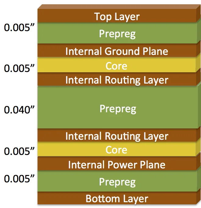
1.1 Stackup Design
Any-Layer HDI: Laser-drilled interconnects across all layers (e.g., 10-layer any-layer in iPhone motherboards).
Sequential Lamination: Multiple lamination cycles for advanced HDI (e.g., 3+N+3 buildup).
1.2 Microvia Fabrication
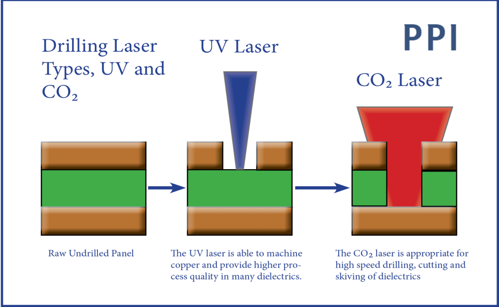
Laser Drilling: CO₂/UV lasers drill sub-50μm vias with ±10μm accuracy.
Via Plating: Electroplated copper or conductive paste ensures via reliability.
1.3 Fine Line Patterning
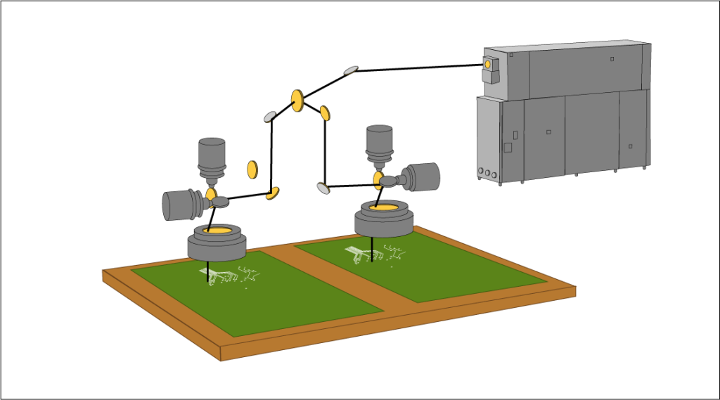
mSAP (Modified Semi-Additive Process): Achieves 2/2μm line width/space on thin copper.
Direct Imaging (DI): Laser-based exposure eliminates phototool misalignment.
2. Materials and Architecture
2.1 Substrate Materials
High-Frequency Laminates: Panasonic MEGTRON 6 (Dk=3.7, Df=0.002) for 5G mmWave antennas.
Ultra-Thin Cores: ≤50μm cores for slim profiles (e.g., smartphone boards).
2.2 Interconnect Structures
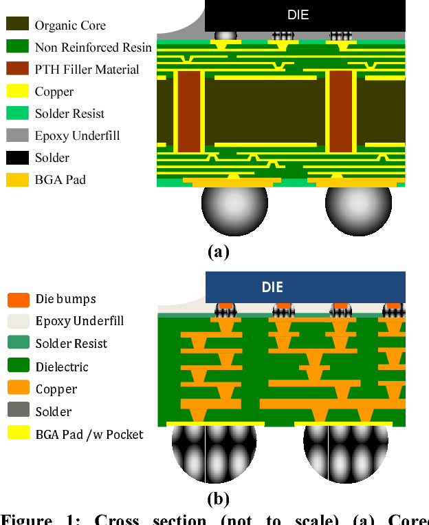
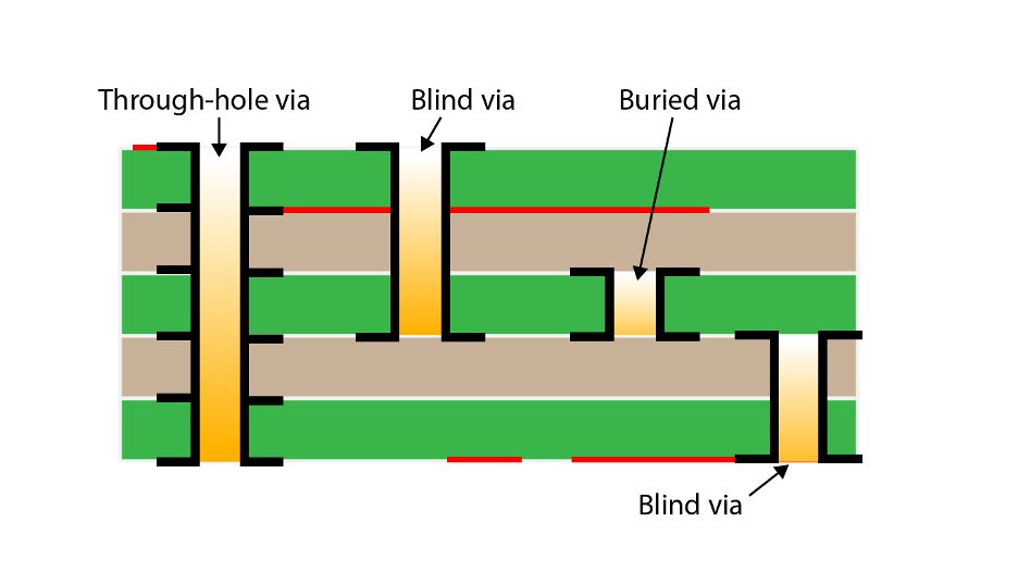
Blind/Buried Vias: Reduce through-hole count, maximize routing space.
Stacked vs. Staggered Vias: Stacked vias increase density but require stress management.
3. Design Challenges
3.1 Signal Integrity
Impedance Control: Use 3D solvers (e.g., Polar SI9000) to compensate via stubs.
Crosstalk Mitigation: Apply via shielding and orthogonal routing.
3.2 Thermal Management
Embedded Heat Spreaders: Integrate copper/graphene layers for localized cooling.
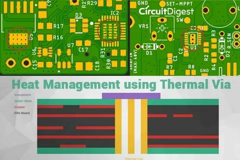
Thermal Via Arrays: Dense micro-vias reduce thermal resistance (e.g., CPU substrates).
3.3 DFM Rules
Annular Ring: ≥75μm to ensure drilling tolerance.
CAF Resistance: Use low-moisture materials (e.g., Isola FR408HR).

4. Modeling and Simulation
4.1 EM Simulation
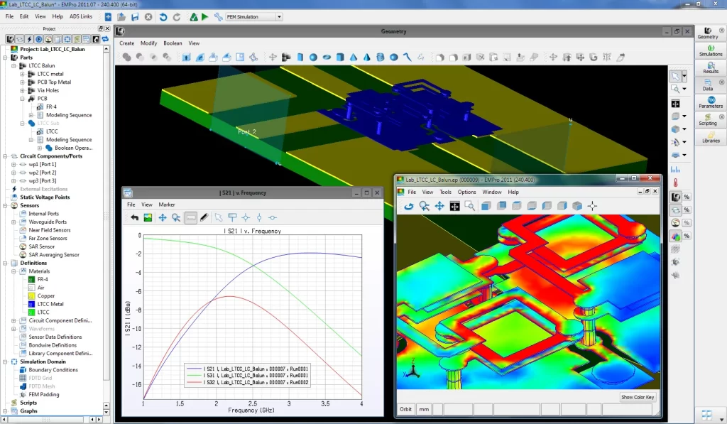
3D Full-Wave Analysis: Validate insertion/return loss for 28Gbps SerDes via HFSS/CST.
Power Integrity: Optimize decoupling networks with PowerSI.
4.2 Mechanical Testing
Thermal Cycling: -55°C to 125°C for 1,000 cycles to assess microvia reliability.
Flexural Testing: Ensure flex HDI durability in foldable devices.
5. Cost Optimization
5.1 Tier Selection
Tier 1 HDI: Single laser drilling for cost-sensitive applications.
Any-Layer HDI: Premium performance for flagship devices.
5.2 Hybrid Materials
FR-4 Mix: Use high-speed materials only in critical layers.
5.3 Panelization
Optimized Layout: Maximize panel utilization to reduce waste.
Conclusion
HDI PCBs are pivotal in driving miniaturization and high-speed performance across industries. Designers must balance density, signal integrity, thermal management, and cost while advancing microvia and material technologies. With the rise of IC substrates, heterogeneous integration, and AIoT, HDI will evolve toward ultra-high density (≤1mil traces), multifunctional integration, and sustainable manufacturing, cementing its role as the backbone of next-gen smart hardware.
Contact
805, Block A, Guangming Centre, No. 2, Chuangming Road, Yongning Street, Zengcheng District, Guangzhou, China
- op@eazypcb.com
- Eazypcb
- +86 13342868540


