Flexible PCB
Manufacturing multilayer PCB up to 56 layer, IPC III Standard, Multilayer Rigid PCB, Multilayer Flex PCB, Rigid-flex Board, hybrid PCB…
Personal Information

Introduction
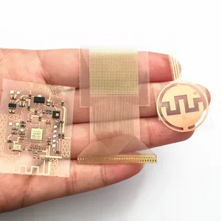
Flexible Printed Circuit Boards (FPCBs), commonly referred to as flex circuits, are a revolutionary type of electronic interconnect solution. Unlike traditional rigid PCBs, FPCBs are designed to bend, twist, and conform to intricate shapes without losing functionality. Their unique properties make them ideal for applications in compact and dynamic environments, such as wearable devices, automotive systems, aerospace equipment, and medical technologies.
Flex PCBs enable manufacturers to reduce product weight, minimize assembly complexity, and improve overall system reliability. As technology evolves, FPCBs are becoming increasingly indispensable in the development of cutting-edge electronic devices.
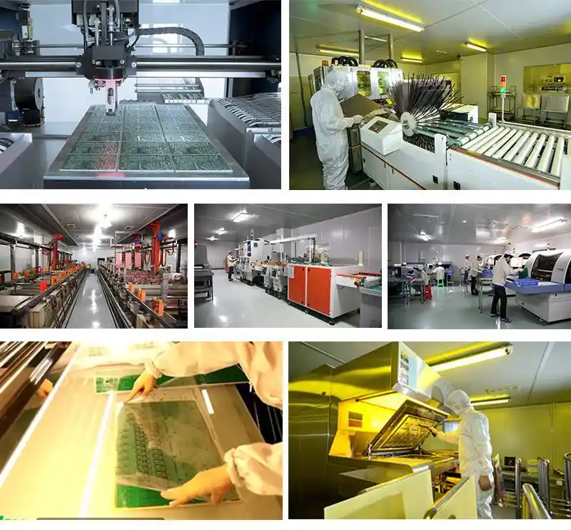
Flexible PCB's Manufacturing Process
The manufacturing process of flexible PCBs is a combination of precision engineering and advanced technology. Key steps include:
Substrate Preparation:
Flexible PCBs use thin layers of polyimide (PI) or polyester (PET) films as substrates due to their flexibility and thermal stability. These films are cleaned and treated to ensure good adhesion.Copper Cladding:
A copper layer is laminated onto the substrate using either adhesive bonding or a direct deposition process. Adhesive-free laminates are preferred for high-performance applications as they offer better thermal and electrical properties.Circuit Patterning:
Photolithography or laser etching is used to define circuit patterns. A photoresist is applied, exposed to UV light through a mask, and developed to leave behind the desired copper paths.Etching and Stripping:
Unnecessary copper is etched away using chemical solutions, leaving only the circuit traces.Drilling and Plating:
Precision drilling methods such as laser drilling create microvias for interconnections. The vias are then plated with copper for conductivity.Coverlay and Finishing:
Protective layers, such as polyimide coverlays or solder masks, are applied to shield the circuit from environmental factors like moisture, dust, and chemicals.Inspection and Testing:
Comprehensive electrical and visual inspections are conducted to ensure quality and reliability.

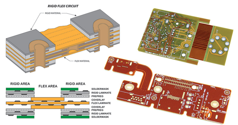
Flexible PCB's Materials and Structure
Flexible PCBs are constructed from specialized materials to meet performance and durability requirements:
Substrate Material:
- Polyimide (PI): Preferred for its excellent thermal resistance and flexibility.
- Polyester (PET): Cost-effective but with lower heat resistance.
Conductive Layer:
- Thin copper foil (electrodeposited or rolled annealed) forms the circuit paths.
Adhesive Layers:
- Acrylic or epoxy adhesives are used to bond layers together. Adhesive-free laminates are used for high-reliability applications to reduce delamination risk.
Coverlay:
- A protective layer (typically polyimide or a flexible solder mask) shields the circuits while allowing for flexibility.
Optional Stiffeners:
- Added in areas requiring rigidity, such as under connectors or components.
This multilayer structure allows FPCBs to flex without compromising electrical performance or mechanical integrity.
Flexible PCB's Design Considerations
Designing flexible PCBs involves specific guidelines to ensure reliability and functionality:
Bend Radius:
- Maintain a minimum bend radius (typically 10 times the thickness of the material) to prevent mechanical stress and cracks.
Trace Routing:
- Avoid sharp angles; use curved traces to minimize stress concentrations.
- Stagger vias and avoid placing them in flexing regions.
Layer Stackup:
- Use balanced copper layers to prevent warping.
Component Placement:
- Place components and connectors away from bending zones.
- Use reinforcement materials like stiffeners for heavy components.
Thermal Management:
- Account for heat dissipation in high-power applications.
Modeling and Analysis
Advanced simulation tools play a crucial role in designing flexible PCBs:
3D CAD Modeling:
Enables engineers to visualize the PCB in its folded or flexed state, ensuring it fits within the product enclosure.Finite Element Analysis (FEA):
Predicts mechanical stresses and evaluates the durability of the flex circuits under repeated bending.Thermal Simulation:
Identifies potential hot spots in high-current applications.
Signal Integrity Considerations
Maintaining signal integrity in flexible PCBs is critical, particularly for high-speed digital and RF designs:
Controlled Impedance Design:
- Ensure uniform trace widths and spacing for signal traces.
Minimizing Crosstalk:
- Use adequate spacing between signal lines and ground planes.
Shielding:
- Add grounded layers or use EMI shielding films for high-frequency designs.
Via Optimization:
- Reduce the number of vias to avoid signal distortion and impedance mismatches.
Cost Considerations
While flexible PCBs are costlier than rigid PCBs, several strategies can help control costs:
Material Selection:
- Choose materials appropriate for the application to avoid unnecessary expenses.
Simplify Design:
- Minimize layers and avoid overcomplicated structures.
Panelization:
- Optimize the layout to reduce material waste during manufacturing.
Conclusion
Flexible PCBs have transformed the electronics industry by enabling innovative designs that were previously impossible with rigid boards. Their adaptability, lightweight structure, and reliability make them ideal for modern electronic devices. By understanding their manufacturing processes, material choices, and design considerations, engineers can unlock their full potential while balancing performance and cost.
Contact
805, Block A, Guangming Centre, No. 2, Chuangming Road, Yongning Street, Zengcheng District, Guangzhou, China
- op@eazypcb.com
- Eazypcb
- +86 13342868540