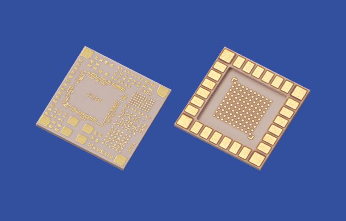
Ceramic PCB
Manufacturing multilayer PCB up to 56 layer, IPC III Standard, Multilayer Rigid PCB, Multilayer Flex PCB, Rigid-flex Board, hybrid PCB…
Personal Information

Introduction
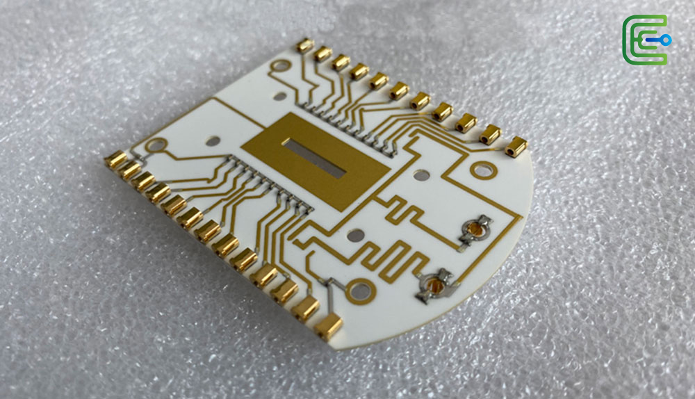
Ceramic PCBs (Printed Circuit Boards) are high-performance substrates made from ceramic materials such as alumina (Al₂O₃), aluminum nitride (AlN), or beryllium oxide (BeO). Designed for extreme temperatures, high-frequency operation, and superior thermal conductivity, they outperform traditional organic substrates (e.g., FR-4) in mechanical strength, CTE matching, and electrical insulation. Widely used in high-power LEDs, automotive electronics, aerospace, and medical devices, this article explores the technical advantages and design practices of ceramic PCBs.
1. Manufacturing Process Overview
Key steps in ceramic PCB fabrication:
Substrate Forming: Mix ceramic powder (e.g., Al₂O₃) with binders, shaped via dry pressing or tape casting.
High-Temperature Sintering: Fire green substrates at >1600°C in inert atmospheres to achieve dense structures.
Metallization: Apply conductive layers via thick-film printing (silver/gold paste) or thin-film processes (sputtering/electroplating).
Laser Cutting: Use UV lasers for precise edge finishing to prevent micro-cracks.
2. Material and Structure
Core material properties:
Substrate Types:
Alumina (Al₂O₃): Cost-effective, thermal conductivity ~24-28 W/m·K for medium-power applications.
Aluminum Nitride (AlN): High thermal conductivity (170-200 W/m·K) for IGBT modules.
Beryllium Oxide (BeO): Ultra-high conductivity (~300 W/m·K) but restricted to military use due to toxicity.
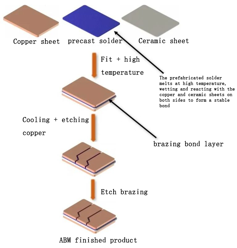
Metallization: Copper, silver, or gold layers bonded via DPC (Direct Plated Copper) or AMB (Active Metal Brazing).
3. Design Considerations
Critical design factors:
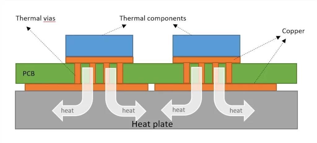
Thermal Management: Simulate heat dissipation paths and optimize power device placement.
CTE Matching: Align ceramic substrate CTE (~6-7 ppm/°C) with solder alloys (e.g., SnAgCu) to prevent thermal fatigue.
High-Frequency Layout: Leverage low dielectric loss (Df<0.001) for mmWave antennas or RF modules.
4. Modeling and Analysis
Simulation methodologies:
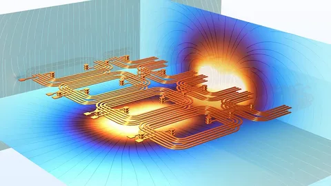
Thermal Analysis: Use ANSYS Icepak/COMSOL to predict junction temperatures and avoid overheating.
Mechanical Stress Testing: Evaluate vibration/shock resistance to prevent brittle fractures.
High-Frequency Modeling: Optimize microstrip/CPW layouts in HFSS to minimize signal loss.
5. Signal Integrity Management
Strategies for high-frequency designs:
Impedance Control: Calculate trace dimensions based on ceramic Dk values (e.g., Al₂O₃ Dk=9-10).
Grounding Techniques: Implement low-inductance ground planes in LTCC multilayer substrates.
Embedded Passives: Integrate resistors/capacitors within ceramic layers to enhance signal stability.
6. Cost Optimization
Cost-reduction approaches:
Hybrid Materials: Use Al₂O₃ for non-critical layers combined with AlN for high-power areas.
Standardization: Adopt common substrate sizes (e.g., 30×30mm DBC boards) to reduce customization costs.
Bulk Purchasing: Negotiate volume discounts with ceramic material suppliers.
Conclusion
Ceramic PCBs are revolutionizing high-power and high-frequency electronics with their unmatched thermal performance and reliability. By balancing material selection, advanced simulations, and cost efficiency, designers can unlock their full potential in EVs, 5G infrastructure, and industrial systems. As wide-bandgap semiconductors (SiC/GaN) gain traction, ceramic substrates will play a pivotal role in enabling next-generation power electronics.
Contact
805, Block A, Guangming Centre, No. 2, Chuangming Road, Yongning Street, Zengcheng District, Guangzhou, China
- op@eazypcb.com
- Eazypcb
- +86 13342868540