Introduction: The Backbone of Electronics
In the world of electronics, Printed Circuit Boards (PCBs) are the silent heroes behind almost every device, from smartphones to industrial machines. Understanding the manufacturing processes behind PCBs is essential for anyone involved in electronics design, production, or procurement.
In this article, we’ll break down 10 essential PCB manufacturing processes that you need to know. Whether you're a novice or an experienced professional, these processes are fundamental to creating high-quality, reliable PCBs for various applications.
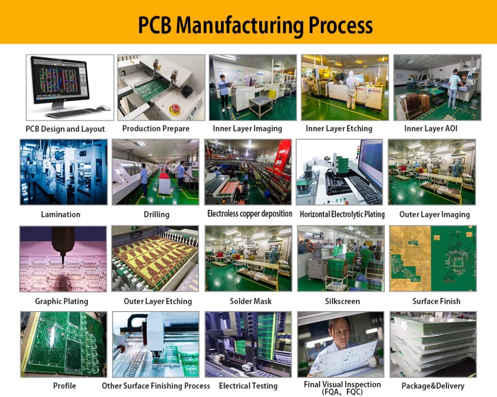 Overview of PCB manufacturing process
1. PCB Design and Schematic Creation
The first step in the PCB manufacturing process is the design stage. Here, engineers create detailed schematics that lay out the electrical connections and components of the PCB. This phase includes specifying the size, layout, and complexity of the board, as well as deciding on component placement and routing.
A good PCB design ensures that electrical signals flow correctly, minimizing interference and preventing errors.
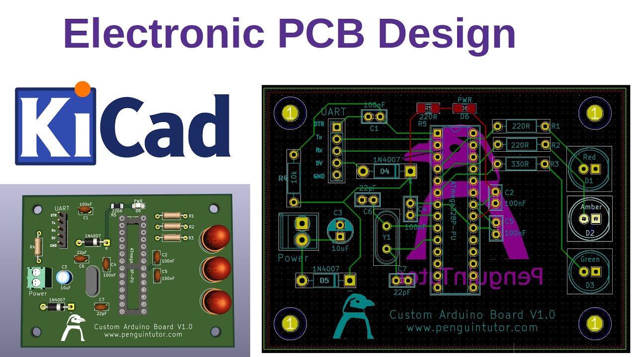 PCB schematic design process
2. PCB Material Selection
After the design is finalized, the next step is selecting the right materials. PCB materials typically consist of a core layer (usually made from fiberglass), copper layers (for conducting electricity), and solder mask (to prevent short circuits). The material choice impacts the performance, cost, and durability of the PCB.
Common materials include FR4, CEM-1, and polyimide, each chosen based on specific project requirements like thermal performance or flexibility.
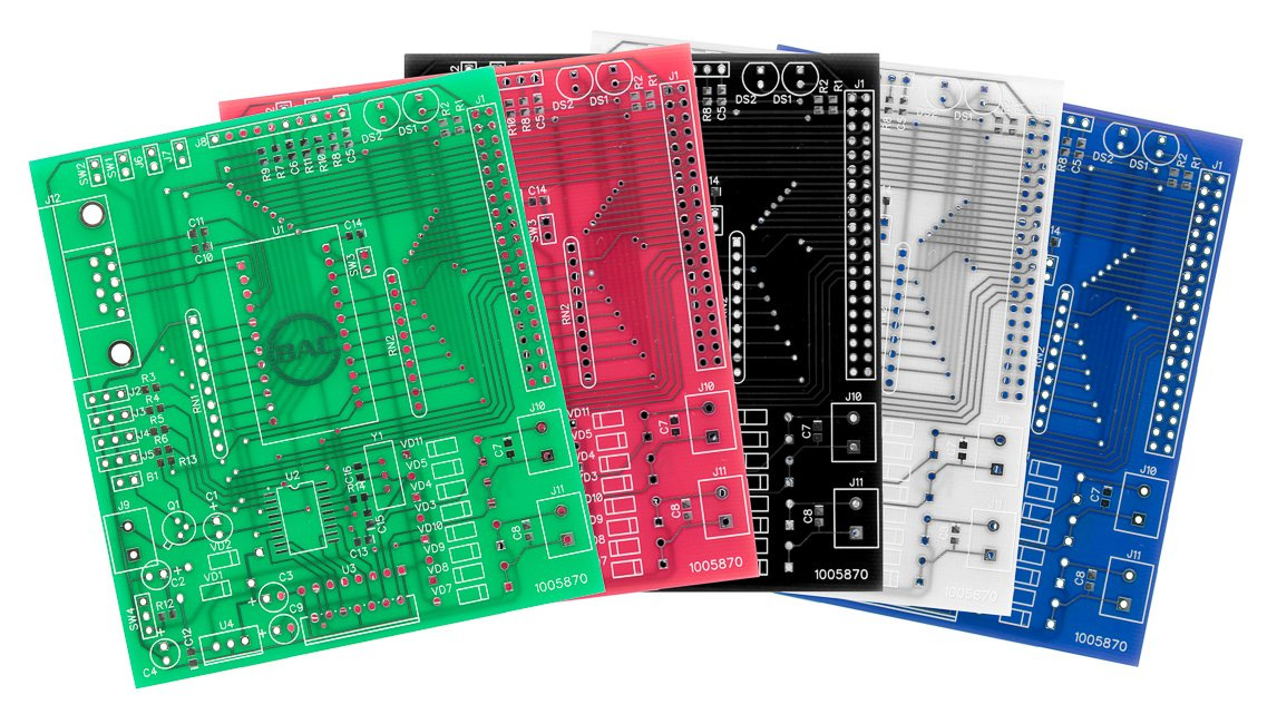 PCB material selection
3. PCB Printing and Etching
Once the materials are selected, the design is transferred onto the PCB through printing. This involves applying a thin layer of copper onto the board and using photolithography or etching techniques to create the circuit pathways. The board is then exposed to UV light to transfer the design from the film to the PCB, followed by a chemical etching process that removes unwanted copper.
This process is critical to ensuring that the copper traces are clean, precise, and free from defects.
 PCB etching process
4. Drilling and Component Hole Creation
In this phase, holes are drilled into the PCB to accommodate through-hole components or vias (small holes that connect different layers of the PCB). The drilling process can be done using lasers or mechanical drills, depending on the complexity and size of the board.
Precision is key here, as improperly drilled holes can cause alignment issues and affect the overall functionality of the PCB.
 PCB drilling process
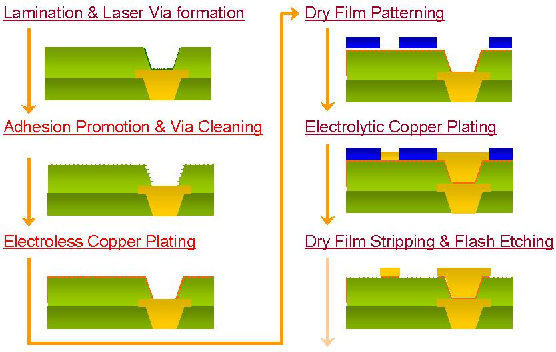
5. Copper Plating
After drilling, copper plating is used to coat the drilled holes with a layer of copper. This process is necessary to form electrical connections between the PCB layers and ensure that the components are properly connected. Electroless copper plating is a commonly used method, followed by electrolytic copper plating for a more robust finish.
Copper plating enhances the board's conductivity, durability, and overall performance.
 PCB copper plating process
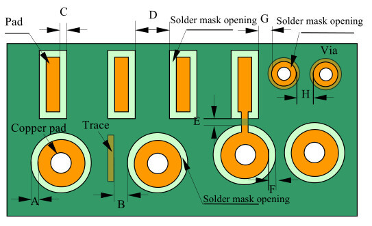
6. Solder Mask Application
After copper plating, the PCB undergoes a solder mask application. This is a protective coating that prevents the solder from flowing onto unintended areas of the board during assembly. The solder mask also acts as a dielectric layer, protecting the board from moisture and environmental damage.
The solder mask is usually green, but other colors can also be used based on the manufacturer’s preference.
 PCB solder mask application
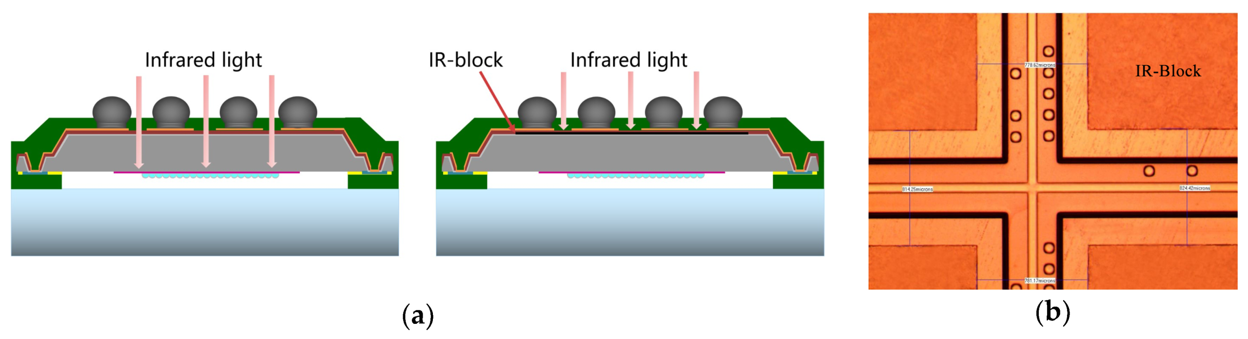
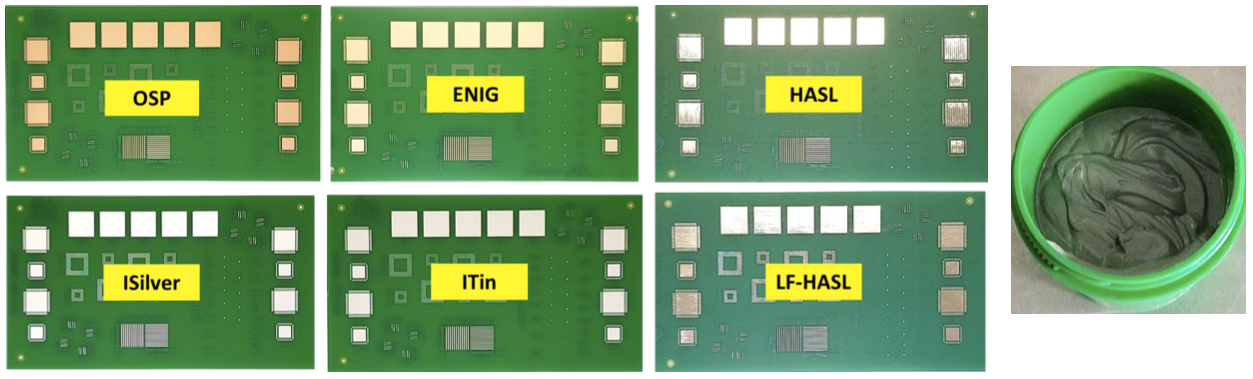
7. Surface Finish and Soldering
To complete the PCB, a surface finish is applied to the exposed copper pads. The surface finish ensures good solderability, which is essential for the efficient attachment of components. Common finishes include HASL (Hot Air Solder Leveling), ENIG (Electroless Nickel Immersion Gold), and OSP (Organic Solderability Preservative).
This process significantly impacts the quality and longevity of the PCB.
 PCB surface finish soldering
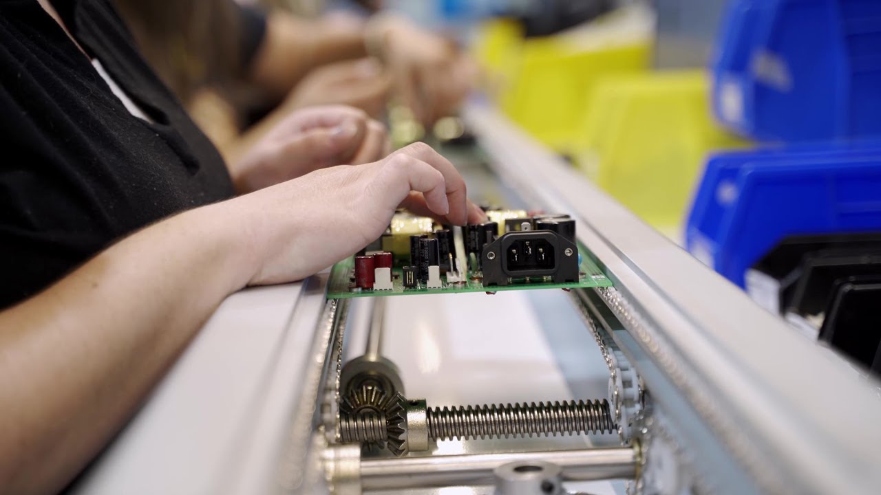
8. PCB Assembly (SMT and THT)
At this stage, components are soldered onto the PCB. This can be done using Surface-Mount Technology (SMT) or Through-Hole Technology (THT), depending on the component type and board design.
- SMT is more common for compact, lightweight components.
- THT is used for larger components that require strong mechanical bonds.
 PCB assembly using SMT and THT
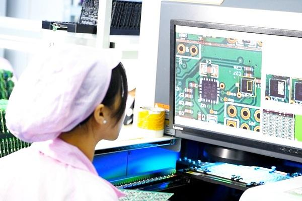
9. Inspection and Testing
After assembly, the PCB goes through several inspection and testing processes. These include visual inspection, Automated Optical Inspection (AOI), and Electrical Testing (ICT) to ensure that all components are placed correctly and that the board functions as intended.
Testing is critical to catch any potential defects or shorts early on, which could lead to malfunctions or failures in the final product.
 PCB inspection and testing
10. Final Assembly and Packaging
The last step involves final assembly and packaging. This stage includes any additional components, such as connectors or heat sinks, and the final packaging for shipment to customers. Conformal coating may also be applied to protect the PCB from environmental factors like moisture and dust.
Once packaged, the PCB is ready for integration into the final product.
 PCB final assembly and packaging
FAQ: Common Questions About PCB Manufacturing
Q1: What’s the difference between SMT and THT?
A1: SMT (Surface Mount Technology) is used for placing components directly on the surface of the PCB, whereas THT (Through-Hole Technology) involves inserting components through holes in the PCB for a stronger connection.
Q2: Can I design a PCB without using a professional CAD tool?
A2: While it’s possible, professional PCB design software provides essential features like error checking and routing optimization, which are difficult to achieve manually.
Conclusion: Mastering the Basics
From design to assembly, mastering these 10 essential PCB manufacturing processes ensures that you can produce high-quality, reliable PCBs that meet your product’s requirements. Understanding each step and its role in the overall process will help you make informed decisions throughout the design and manufacturing phases.
Whether you're designing a PCB for the first time or working with experienced manufacturers, knowledge of these processes is essential for success in the electronics industry.